 Copyright © Michael Richmond.
This work is licensed under a Creative Commons License.
Copyright © Michael Richmond.
This work is licensed under a Creative Commons License.
The basic CCD
Much of this material is taken wholesale from
a presentation by
Simon Tulloch,
an astronomer at the
European Southern Observatory.
Simon has kindly granted me permission to use this material --
thanks, Simon!
Another good overview is given by the article Charge Coupled Devices in Astronomy by Craig Mackay, in Annual Reviews of Astronomy and Astrophysics, vol 24, p. 255 (1986).
The photoelectric effect is fundamental to the operation of a CCD. Atoms in a silicon crystal have electrons arranged in discrete energy bands. The lower energy band is called the Valence Band, the upper band is the Conduction Band. Most of the electrons occupy the Valence band but can be excited into the conduction band by heating or by the absorption of a photon. The energy required for this transition is 1.26 electron volts. Once in this conduction band the electron is free to move about in the lattice of the silicon crystal. It leaves behind a "hole" in the valence band which acts like a positively charged carrier. In the absence of an external electric field the hole and electron will quickly re-combine and be lost. In a CCD an electric field is introduced to sweep these charge carriers apart and prevent recombination.

Thermally generated electrons are indistinguishable from photo-generated electrons. They constitute a noise source known as "Dark Current" and it is important that CCDs are kept cold to reduce their number.
   The band gap energy of silicon is 1.26 eV.  Photons with
   less energy cannot knock an electron free from an atom.


   Q:  What is the wavelength of a photon corresponding
          to this critical energy?
At longer wavelengths, silicon becomes transparent to light and CCDs constructed from silicon become insensitive.
First, watch this little animation ... we'll go over the steps in detail in a moment.

First, we open the shutter and let rain (light) fall on the array, filling the buckets (pixels). At the end of the exposure, we close the shutter.
Now, shift the buckets along the conveyor belts.

Dump the first set of buckets into the special conveyor belt (the serial register) at the end of the array.

Now, leave the ordinary conveyor belts fixed for a moment, and start to shift the special conveyor belt so that the first bucket empties into the graduated cylinder (readout amplifier).


Record the amount of water (charge) in this first bucket, then shift the special conveyor belt again to bring the second bucket to the graduated cylinder.


Record this bucket's contents, too, and then repeat until we've read all the buckets on the special conveyor belt.


Now, with a fresh set of empty buckets on the special conveyor belt, move the main conveyor belts forward again to bring the next row of buckets to the edge of the array.

Dump the next set of buckets into the special conveyor belt.

Now, leave the ordinary conveyor belts fixed again, and start to shift the special conveyor belt so that its first bucket empties into the graduated cylinder.


Record the amount of water in this first bucket, then shift the special conveyor belt again to bring the second bucket to the graduated cylinder.


Record this bucket's contents, too, and then repeat until we've read all the buckets on the special conveyor belt.


Repeat this procedure until all the bucket have been shifted to the special conveyor belt and dumped one by one into the graduated cylinder.
Below is a view of the procedure in action, showing a small image gradually being shifted and transferred down the chip as it is read out.

Note that as the image is shifted and read out, it disappears from the chip. This means that in CCDs, all readouts are destructive: they destroy the pattern of electrons (based on the pattern of light) as the information is gathered. That means that there is no way to check on the progress of a long exposure; if you guessed the wrong exposure time, you might saturate your target and have to start all over again.
But how does this all happen? How are electrons moved from one location to another inside the silicon?
The diagram below shows a small section (a few pixels) of the image area of a CCD. This pattern is repeated. Note that a single pixel contains three electrodes (horizontal rows), not just one. That is very important, as you will soon see.

Every third electrode is connected together. Bus wires running down the edge of the chip make the connection. The channel stops are formed from high concentrations of Boron in the silicon.
Once again every third electrode is in the serial register connected together. Below the image area (the area containing the horizontal electrodes) is the "Serial register". This also consists of a group of small surface electrodes. There are three electrodes for every column of the image area

In the photomicrograph of an EEV CCD below, the serial register is bent double to move the output amplifier away from the edge of the chip. This useful if the CCD is to be used as part of a mosaic. The arrows indicate how charge is transferred through the device. Click on the image to see a bigger photograph.

Now, the fact that ALL the pixels in a CCD are measured by a single amplifier can be both a Good Thing, and a Bad Thing.
      Q:  I have used a camera based on the  e2V CCD 231-84
      chip, which has 4096 x 4096 pixels.  If the readout time per pixel
      is t = 2.2 μs, how long does it take to read out the entire chip?
The n-type layer contains an excess of electrons that diffuse into the p-layer. The p-layer contains an excess of holes that diffuse into the n-layer. This structure is identical to that of a diode junction. The diffusion creates a charge imbalance and induces an internal electric field. The electric potential reaches a maximum just inside the n-layer, and it is here that any photo-generated electrons will collect. All science CCDs have this junction structure, known as a "Buried Channel". It has the advantage of keeping the photo-electrons confined away from the surface of the CCD where they could become trapped. It also reduces the amount of thermally generated noise (dark current).

During integration of the image, one of the electrodes in each pixel is held at a positive potential. This further increases the potential in the silicon below that electrode and it is here that the photoelectrons are accumulated. The neighboring electrodes, with their lower potentials, act as potential barriers that define the vertical boundaries of the pixel. The horizontal boundaries are defined by the channel stops.

It helps to understand the remainder of the process if we rotate the diagram so that photons arrive from above the chip -- so that they look as if they are coming from the sky.

Photons entering the CCD create electron-hole pairs. The electrons are then attracted towards the most positive potential in the device where they create "charge packets". Each packet corresponds to one pixel.

In CCDs, we need to move -- yes, physically move -- electrons from one location on the chip to another, so that they will eventually go to the readout amplifier; there, they will be counted. However, we need to keep all the electrons from pixel A separated from those in neighboring pixel B during this journey; otherwise, we won't know how many photons fell on pixel A and how many on pixel B.
   Q:  Electrons are negatively charged.  Is there some way
           to exert forces on electrons in order to "herd"
           them in a particular direction?
Of course there is! We can use voltages to exert forces on the electrons: positive voltages will attract them, and negative voltages will repel them.
In the following few slides, the implementation of the "conveyor belts" as actual electronic structures is explained. The charge is moved along these conveyor belts by modulating the voltages on the electrodes positioned on the surface of the CCD. The electrodes are grouped so that every third electrode shares the same voltage.
![]()
  Q:  Why are all the electrons clumped together in a small pool
           within each pixel?  Why don't they spread out horizontally?
Now, watch as the voltages supplied to the electrodes change, and the electron packets move in response.
![]()
![]()
![]()
![]()
![]()
![]()
![]()
At the end, we have moved all the charge packets over one pixel, and the voltages are back where they started. By repeating the sequence of voltage changes, we can move the packets another pixel down the column.
Now, exactly how should we orient the chip? In order to corral the electrons properly, the electrodes must sit close to the region in which photons are absorbed. The simplest way to make this happen is to let the photons fly THROUGH the electrodes, from "above" the chip. This is called a front-side illuminated design.

Image courtesy of
Vik Dhillon
Of course, that means that some of the photons may bounce off the electrodes, so this simple design throws away some of the precious light from our targets.
We can avoid that loss if we turn the chip upside-down, so that the electrodes are underneath the silicon, and allow photons to shine onto the "back" of the chip.

Image courtesy of
Vik Dhillon
A backside-illuminated chip will have higher quantum efficiency, but suffers from a couple of annoying issues:
But for some applications, all that extra hassle and expense may be worthwhile:

Chart of QE for different chips courtesy of
Apogee Instruments
Is there a big difference in price between front-illuminated and back-illuminated chips? Let's find out.
Complementary Metal Oxide Semiconductor (CMOS) imaging sensors are very similar to CCDs in most ways.
The big difference is how the pool of electrons knocked free within each pixel is turned into a signal. In CCDs, the entire pool is shifted across the chip, from one pixel to the next ... before finally reaching a single amplifier; there, the electrons are finally "counted". Among the important consequences are that it can take a long time to read out a big chip, since millions of pixels all must be processed by a single amplifier; and that the pool of electrons from each pixel is discarded after having been measured.
But in CMOS devices, each pixel is not simply an tiny volume of silicon, inside which electrons sit and wait. Instead, each pixel is manufactured with its own amplifier, allowing it to read its own charge without having to move the electrons. This additional circuitry is the origin of the term active pixel sensor, which is sometimes applied to these devices.

Image courtesy of
Stefano Meroli's blog
That means that a CMOS chip is more complicated to create, certainly, but does give it some advantages over the CCD (as well as a few disadvantages):
This allows one to use different algorithms to determine the charge in a pixel, which might lead to better results; it also permits one to check an image in the middle of a long exposure.
If one doesn't move the pool, then one suffers from no CTE.
There are a few drawbacks with CMOS devices, of course. For example, because each pixel has its own amplifier, there can be small differences in the conversion of charge to voltage (and hence to output signal) from one pixel to another. A CMOS sensor which is front-illuminated will have a smaller light-collecting area than a similar CCD, because the additional circuitry blocks some of the light which would otherwise land in each pixel.
Still, if you look at the (low-cost) amateur astronomical camera market these days, you will see little difference between the sensitivity of CCD and CMOS cameras.

Image modified slightly from
Pavel Pech's blog
These days, CMOS chips appear to be favored by big manufacturers for the most common applications: ordinary digital cameras, smartphones, industrial imaging. It is likely that CMOS sensors will continue to improve over the next decade.
KIDS - the sensor of the future?
One common feature of both CCDs and CMOS sensors -- when they are used in the optical regime -- is that they convert each optical photon to a single electron. Whether the photon is blue, green, or red, it knocks one electron free to roam through the silicon crystal.
Q: What about the interaction of CCDs with X-rays?
Recently, some astronomers have touted the possibilities of a very different sort of detector, one which is based on a completely different sort of technology. Microwave Kinetic Inductance DeviceS (MKIDS, or KIDS for short) were originally developed with millimeter and sub-millimeter radio waves in mind, but they can be adapted to measure optical and near-IR photons as well. One reason that some scientists would like to use KIDS is that they CAN provide some energy information for each photon that strikes them. Just think: a digital sensor with linear response and short readout time, which provides both an image and a spectrum at the same time!

Figure 2 taken from
Romani et al., ApJ 521L, 153 (1999)
I am NOT a solid-state physicist (or even a physicist, really), so the details of exactly how these sensors work is beyond me. The ultra-simplified idea goes something like this:
The lifetime of the quasi-particles can be very short -- between 10-3 and 10-7 seconds -- which means that IF we can read out our device very rapidly, we might be able to detect each photon as it strikes the detector.
One clever trick is to design each pixel of a device so that it has a slightly different resonant frequency; by sending a "comb" of many, many slightly different frequencies into the device, one can probe each pixel simultaneously. "Reading" all those pixels then becomes a matter of examining the output at each frequency.
By modifying the composition and thickness of the materials used to build the micro-circuits within each pixel, one can change the frequency response of the device to suit one's needs. With suitable choices for the materials, a single device can respond to light over a range of one or two decades in frequency (or wavelength).
Let's look at one particular device: ARCONS (the Array Camera for Optical to Near-infrared Spectrophotometry). This detector looks sort of like a typical CCD camera at first glance

Figure 2 taken from
O'Brien et al., IAUS, 285, 385 (2012)
but if you zoom in, you see that each pixel has a lot inside:

Figure 3 taken from
O'Brien et al., IAUS, 285, 385 (2012)
Each of these pixels is about 222 microns on a side, but the section labelled "TiN Inductor" is the only region of the pixel which responds to light.
  Q:  What fraction of each pixel is filled by the inductor?


  Q:  Is this a problem for overall quantum efficiency?


  Q:  Is there any way to fix this problem?
The total array size is 44 x 46 pixels -- so it's not all that big. And not all of the pixels work properly.

Figure 10 taken from
O'Brien et al., IAUS, 285, 385 (2012)
The quasiparticle lifetime in ARCONS is about 50 microseconds, and ARCONS should be able to record the time of arrival of each photon to about 2 microseconds.
  Q:  How many photons can strike each pixel per second
          before they start to "collide" with each other,
          causing the device to lose energy resolution?
ARCONS achieves a spectral resolution of roughly R = 10 in the visible part of the spectrum. That means that

  Q:  How does this compare to the "spectral resolution"
          of a typical broadband filter, such as Johnson V?
Perhaps this figure will give you a clue ...
The quantum efficiency of ARCONS is shown below -- compare the dotted black line (ARCONS only in the lab) to that of other sensors.

Figure 12 taken from
O'Brien et al., IAUS, 285, 385 (2012)
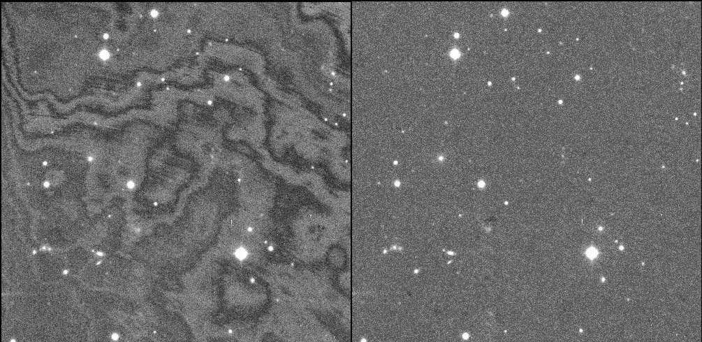
Compare this image of Arp 147 taken by ARCONS on the 200-inch Mt. Palomar telescope to that taken by HST in the inset. The ARCONS image was created by combining 36 exposures of 1 minute each, and using the energy information from each photon to create an RGB color code. Not bad, is it?

Figure 14 taken from
O'Brien et al., IAUS, 285, 385 (2012)
A more recent astronomical device based on MKID technology is the MKID Exoplanet Camera (MEC), which is mounted on the Subaru Telescope, as part of the Subaru Coronographic Extreme Adaptive Optics (SCExAO) package.
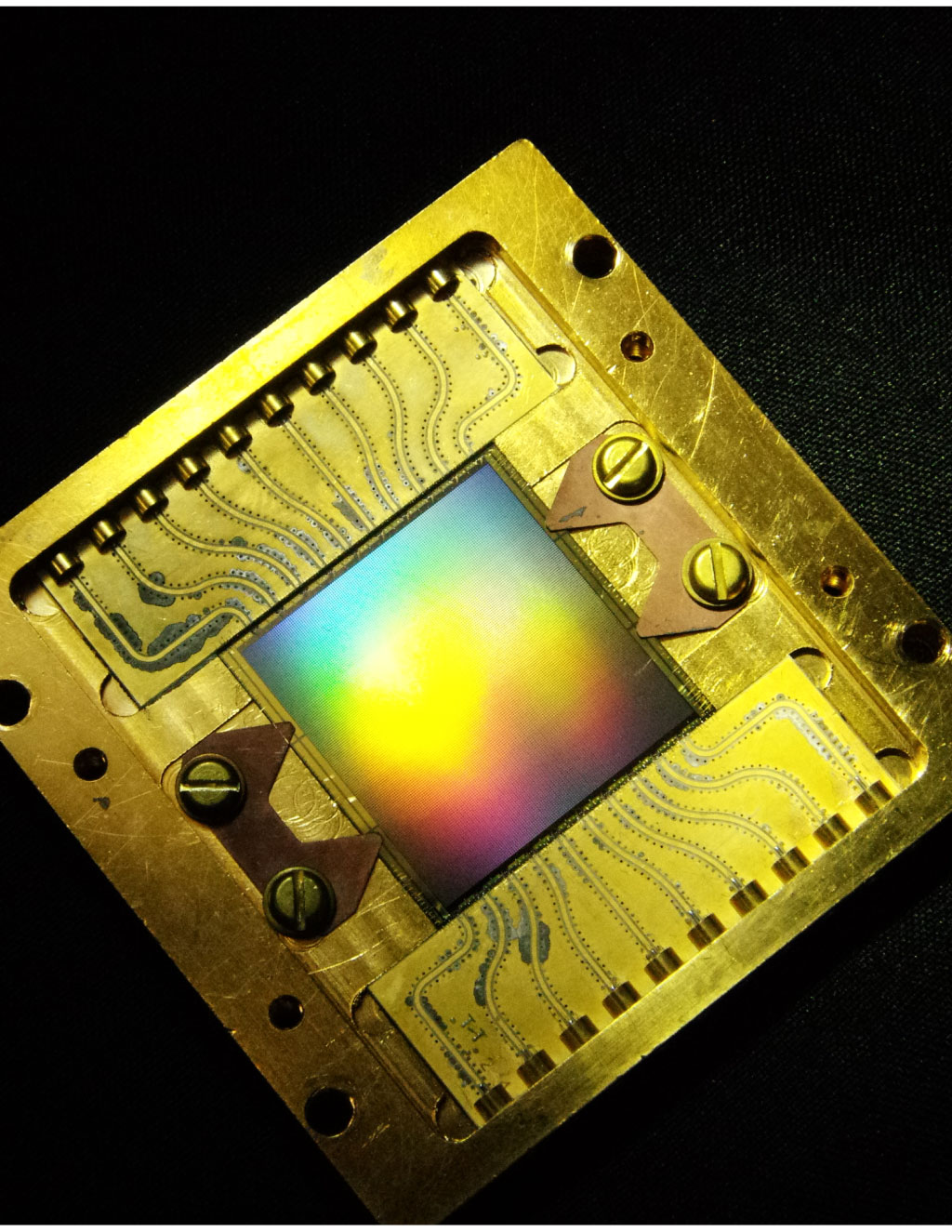
Image courtesy of
NAOJ
This device is used to look at the regions very close to nearby stars in order to find exoplanets; the camera is mounted behind an adaptive optics package which creates very sharp stellar images, allowing the light of the star to be subtracted accurately.
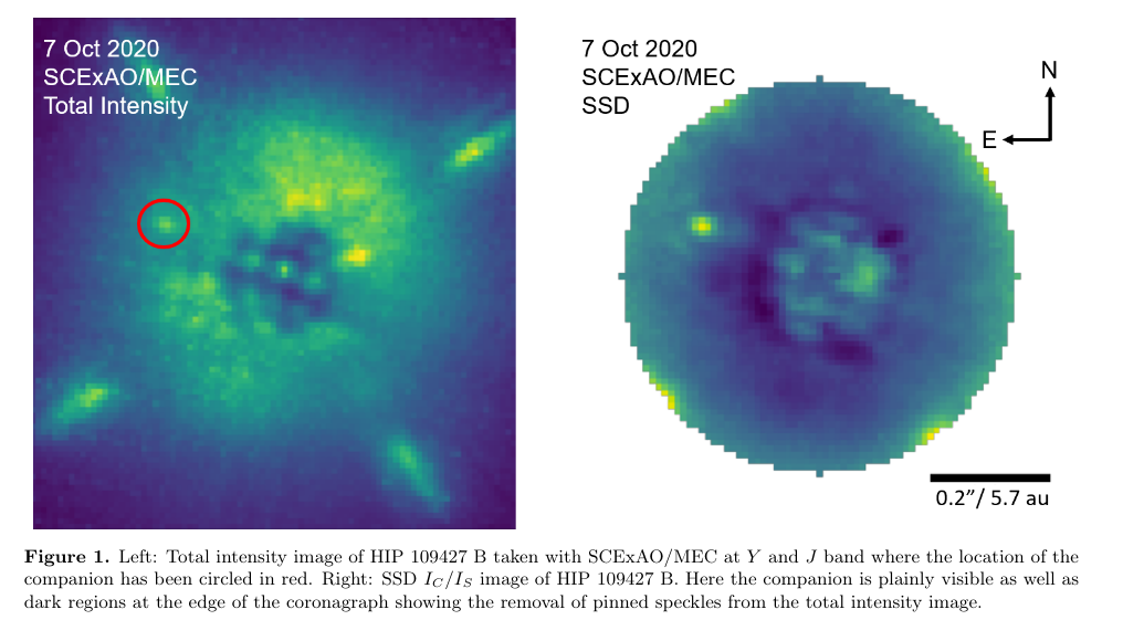
Figure 1 taken from
Steiger et al., AJ 162, 44 (2021)
Why choose an MKID device for this particular job? The authors of Steiger et al., AJ 162, 44 (2021) explain their reasons (I've added emphasis near the end):
A significant improvement over existing systems can be achieved by using read-noise free time domain information on short enough timescales to sample and control, or remove in post-processing, the fast speckle fluctuations from imperfections in the AO system and non-common path aberrations. We have constructed the MKID Exoplanet Camera (MEC) for Subaru Telescope's SCExAO system for this purpose - to serve as both a photon counting, energy resolving science camera, and as a focal plane wavefront sensor to correct for chromatic wavefront errors not accounted for by the upstream AO system. To achieve this, a high-speed, noise-free detector is required, like the Microwave Kinetic Inductance Detector (MKID) array used by MEC.
Now, in my opinion, there's just one problem looming over the development of KIDS for astronomy. That little issue of superconducting means that the detector must be cooled to below 2 degrees Kelvin. As you can see below, machines that can produce temperatures this low tend to be both large and heavy ... not to mention expensive.

Parts of a dilution refrigerator for
a detector developed at CalTech
Copyright © Michael Richmond.
This work is licensed under a Creative Commons License.