
Electric Field in a CCD 1.
The n-type layer contains an excess of electrons that
diffuse into the p-layer. The p-layer contains an
excess of holes that diffuse into the n-layer. This
structure is identical to that of a diode junction.
The diffusion creates a charge imbalance and induces an
internal electric field. The electric potential
reaches a maximum just inside the n-layer, and it is
here that any photo-generated electrons will collect.
All science CCDs have this junction structure, known as
a ‘Buried Channel’. It has the advantage of
keeping the photo-electrons confined away from the
surface of the CCD where they could become trapped.
It also reduces the amount of thermally generated noise
(dark current).
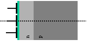


Potential along this line shown
in graph above.


Cross
section through the thickness of the CCD