 Copyright © Michael Richmond.
This work is licensed under a Creative Commons License.
Copyright © Michael Richmond.
This work is licensed under a Creative Commons License.
http://www.ing.iac.es/~smt/CCD_Primer/CCD_Primer.htmSimon has kindly granted me permission to use this material -- thanks, Simon!
Another good overview is given by the article Charge Coupled Devices in Astronomy by Craig Mackay, in Annual Reviews of Astronomy and Astrophysics, vol 24, p. 255 (1986).
CCDs work by converting light into a pattern of electronic charge in a silicon chip. This pattern of charge is converted into a video waveform, digitised and stored as an image file on a computer.
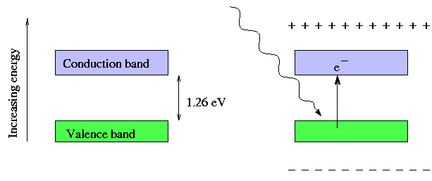
The photoelectric effect is fundamental to the operation of a CCD. Atoms in a silicon crystal have electrons arranged in discrete energy bands. The lower energy band is called the Valence Band, the upper band is the Conduction Band. Most of the electrons occupy the Valence band but can be excited into the conduction band by heating or by the absorption of a photon. The energy required for this transition is 1.26 electron volts. Once in this conduction band the electron is free to move about in the lattice of the silicon crystal. It leaves behind a "hole" in the valence band which acts like a positively charged carrier. In the absence of an external electric field the hole and electron will quickly re-combine and be lost. In a CCD an electric field is introduced to sweep these charge carriers apart and prevent recombination.
Thermally generated electrons are indistinguishable from photo-generated electrons. They constitute a noise source known as "Dark Current" and it is important that CCDs are kept cold to reduce their number.
1.26eV corresponds to the energy of light with a wavelength of 1 micron. Beyond this wavelength silicon becomes transparent and CCDs constructed from silicon become insensitive.
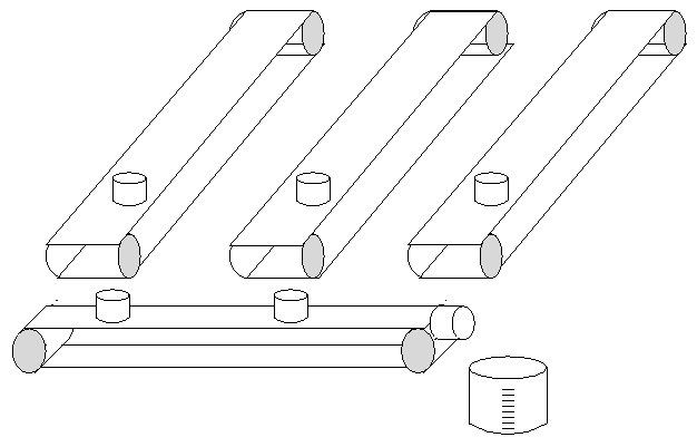
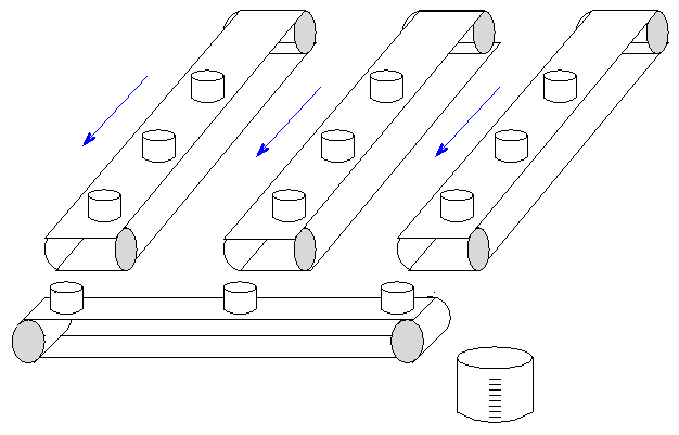
First, we open the shutter and let rain (light) fall on the array, filling the buckets (pixels). At the end of the exposure, we close the shutter.
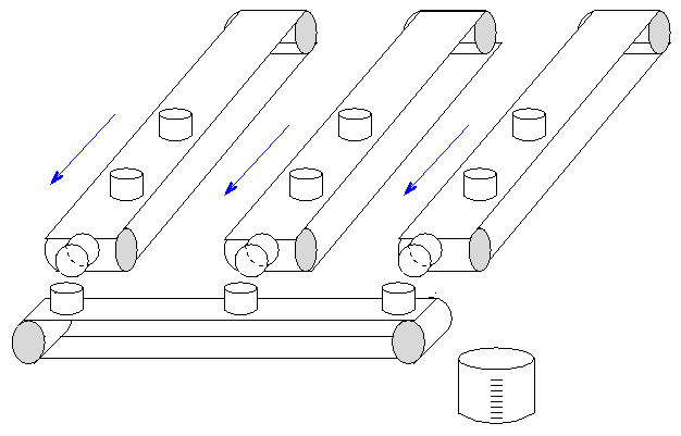
Now, shift the buckets along the conveyor belts.

Dump the first set of buckets into the special conveyor belt (the serial register) at the end of the array.
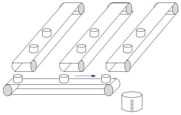
Now, leave the ordinary conveyor belts fixed for a moment, and start to shift the special conveyor belt so that the first bucket empties into the graduated cylinder (readout amplifier).

Record the amount of water (charge) in this first bucket, then shift the special conveyor belt again to bring the second bucket to the graduated cylinder.
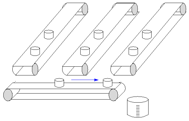

Record this bucket's contents, too, and then repeat until we've read all the buckets on the special conveyor belt.

Now, with a fresh set of empty buckets on the special conveyor belt, move the main conveyor belts forward again to bring the next row of buckets to the edge of the array.
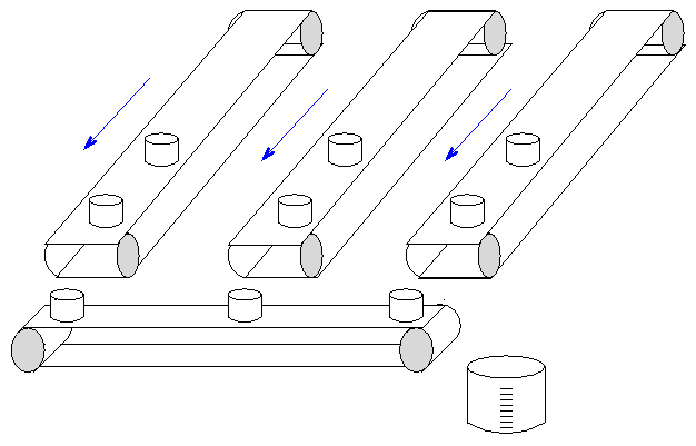
Dump the next set of buckets into the special conveyor belt.

Now, leave the ordinary conveyor belts fixed again, and start to shift the special conveyor belt so that its first bucket empties into the graduated cylinder.
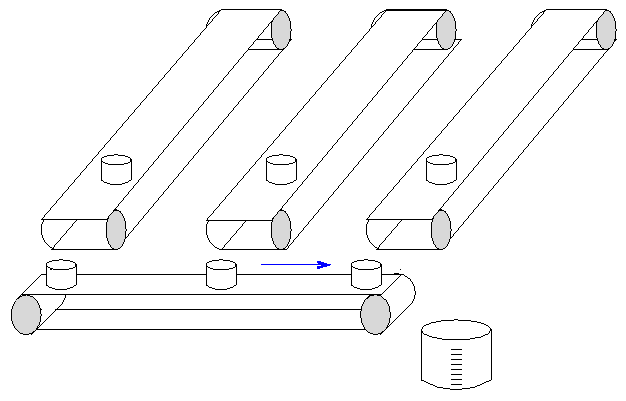
Record the amount of water in this first bucket, then shift the special conveyor belt again to bring the second bucket to the graduated cylinder.


Record this bucket's contents, too, and then repeat until we've read all the buckets on the special conveyor belt.
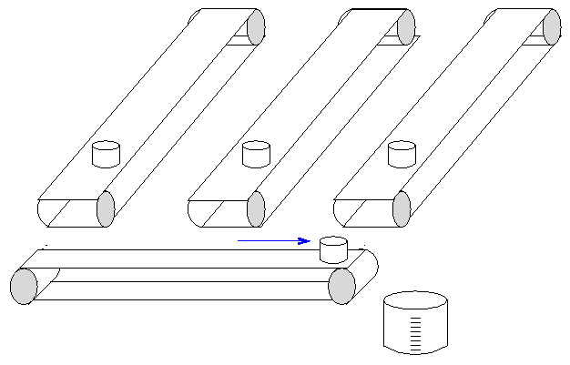
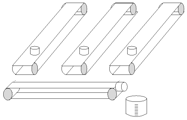
Repeat this procedure until all the bucket have been shifted to the special conveyor belt and dumped one by one into the graduated cylinder.
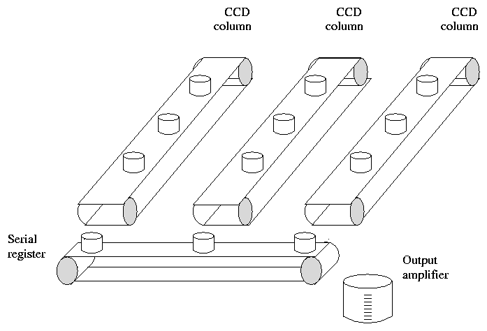
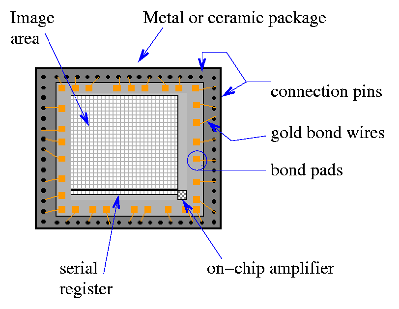
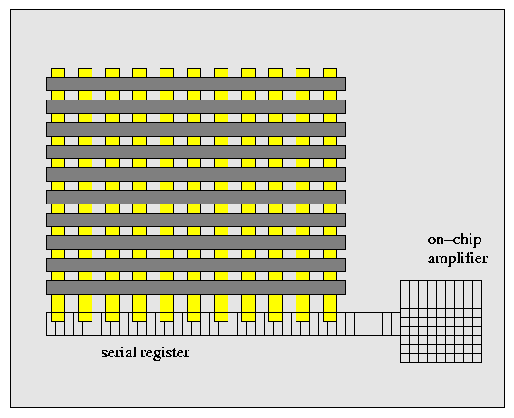
The image area of the CCD is positioned at the focal plane of the telescope. An image then builds up that consists of a pattern of electric charge. At the end of the exposure this pattern is then transferred, one pixel at a time, by way of the serial register to the on-chip amplifier. Electrical connections are made to the outside world via a series of bond pads and thin gold wires positioned around the chip periphery.
CCDs are are manufactured on silicon wafers using the same photo-lithographic techniques used to manufacture computer chips. Scientific CCDs are very big, so only a few can be fitted onto a wafer. This is one reason that they are so costly. The photo below shows a silicon wafer with three large CCDs and assorted smaller devices. A CCD has been produced by Philips that fills an entire 6 inch wafer! It is the worlds largest integrated circuit.

The diagram below shows a small section (a few pixels) of the image area of a CCD. This pattern is repeated.
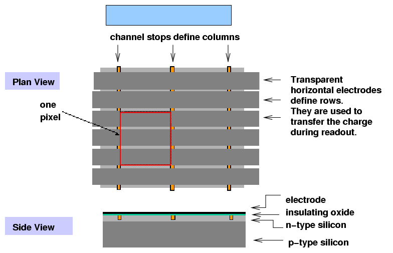
Every third electrode is connected together. Bus wires running down the edge of the chip make the connection. The channel stops are formed from high concentrations of Boron in the silicon.
Once again every third electrode is in the serial register connected together. Below the image area (the area containing the horizontal electrodes) is the "Serial register". This also consists of a group of small surface electrodes. There are three electrodes for every column of the image area
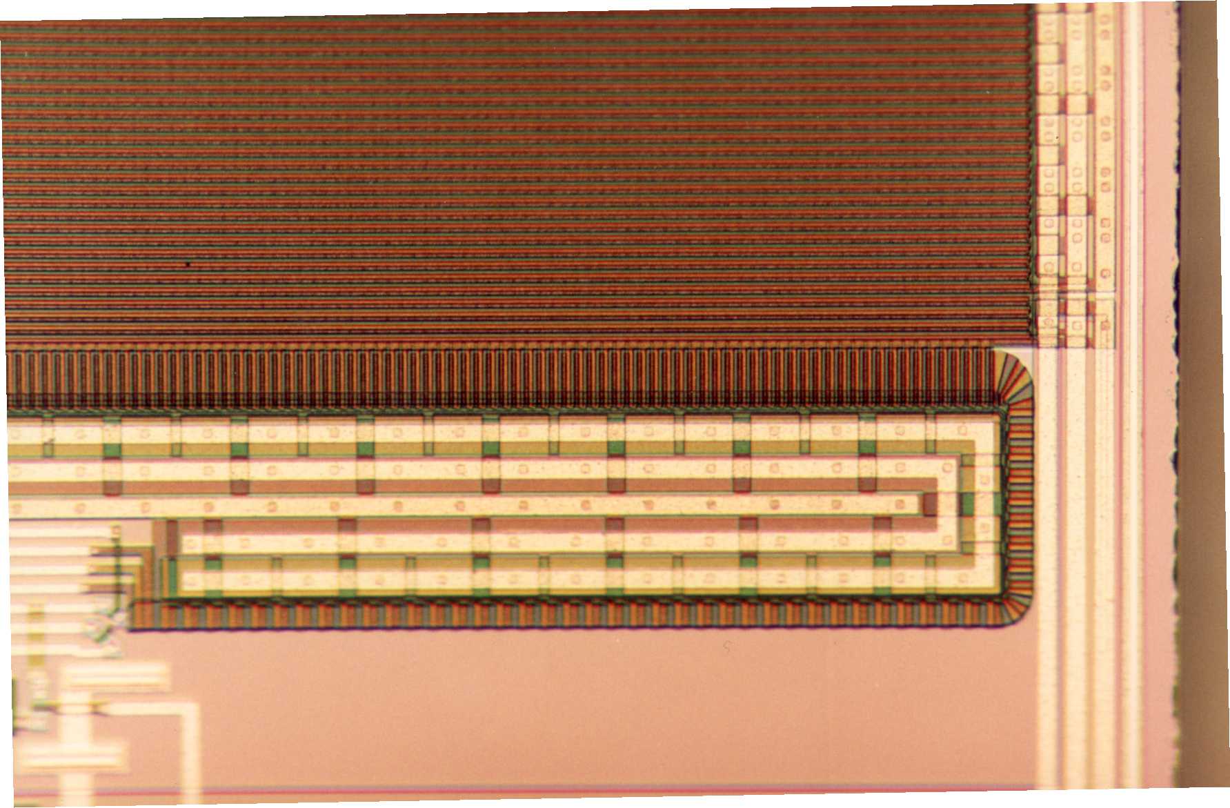
In the photomicrograph of an EEV CCD below, the serial register is bent double to move the output amplifier away from the edge of the chip. This useful if the CCD is to be used as part of a mosaic. The arrows indicate how charge is transferred through the device. Click on the image to see a bigger photograph.
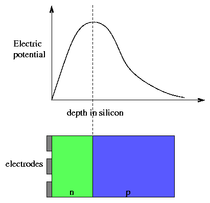
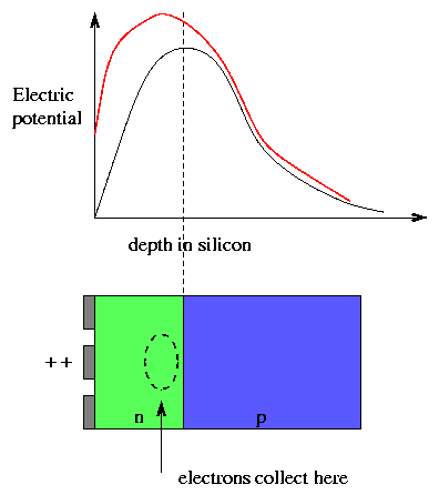
The n-type layer contains an excess of electrons that diffuse into the p-layer. The p-layer contains an excess of holes that diffuse into the n-layer. This structure is identical to that of a diode junction. The diffusion creates a charge imbalance and induces an internal electric field. The electric potential reaches a maximum just inside the n-layer, and it is here that any photo-generated electrons will collect. All science CCDs have this junction structure, known as a "Buried Channel". It has the advantage of keeping the photo-electrons confined away from the surface of the CCD where they could become trapped. It also reduces the amount of thermally generated noise (dark current).
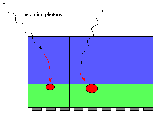
During integration of the image, one of the electrodes in each pixel is held at a positive potential. This further increases the potential in the silicon below that electrode and it is here that the photoelectrons are accumulated. The neighboring electrodes, with their lower potentials, act as potential barriers that define the vertical boundaries of the pixel. The horizontal boundaries are defined by the channel stops.
Photons entering the CCD create electron-hole pairs. The electrons are then attracted towards the most positive potential in the device where they create "charge packets". Each packet corresponds to one pixel.
![]()
Now, watch as the voltages supplied to the electrodes change, and the electron packets move in response.
![]()
![]()
![]()
![]()
![]()
![]()
![]()
At the end, we have moved all the charge packets over one pixel, and the voltages are back where they started. By repeating the sequence of voltage changes, we can move the packets another pixel down the column.
Copyright © Michael Richmond.
This work is licensed under a Creative Commons License.