 Copyright © Michael Richmond.
This work is licensed under a Creative Commons License.
Copyright © Michael Richmond.
This work is licensed under a Creative Commons License.
It's time to start observing our targets! Let's work out a plan for our first night: Wed, Mar 4/5.
Much of the material in this lecture is borrowed from Simon Tulloch at the Isaac Newton Group of Telescopes in La Palma, Spain. You can see his original work in Powerpoint form on the Web at
https://www.ing.iac.es//~eng/detectors/CCD_Info/CCD_Primer.htmSimon has kindly granted me permission to use this material -- thanks, Simon!
I've been telling you for a while now that CCDs are wonderful sensors -- and they are! But they aren't perfect. Today, we'll look at some of the ways that these electronic devices can yield imperfect images. In some cases, we can remove or at least minimize the noise introduced to our measurements by these imperfections.
Many of these imperfections are shared by CMOS sensors. I'll mention the differences when appropriate.
CCDs are not perfect detectors -- they do not record every single photon which strikes them. One reason is the change of index of refraction between air and the silicon itself.
Look at the chips below. Which chips absorb the largest amount of light?
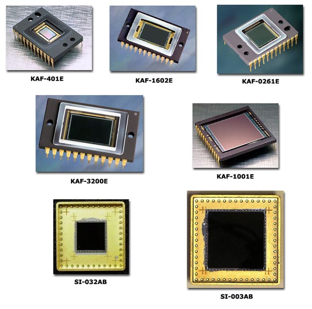
Images of CCD chips courtesy of
astrosurf.com
One can reduce reflective losses by anti-reflection coatings. The idea is to cause destructive interference between a light ray which bounces off the front surface of the coating (labelled "A" in the diagram below) and a light ray which bounces off the back surface of the coating. If we can arrange it so that these reflected light rays interfere correctly, we can in essence prevent such reflection from taking place.
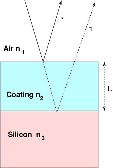
The first ray, "A", has its phase shifted by half a wavelength because it is bouncing off a material with higher refractive index than air. If we can cause the second ray, "B", to have an overall phase shift of zero, then the two rays will be perfectly out of phase and destroy each other.
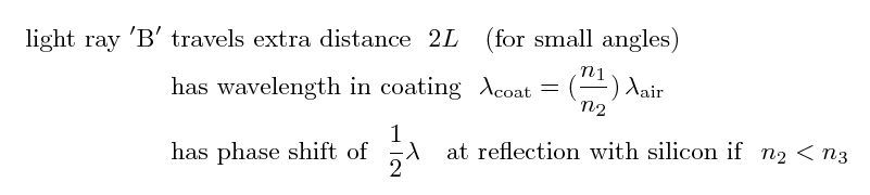
So, in order to create destructive interference between rays "A" and "B", we want
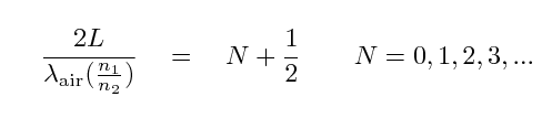
and so
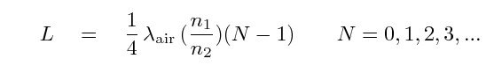
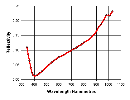
Note that one can arrange for perfect destructive interference only at a particular wavelength; there will be some reflection at other wavelengths. For CCDs, the designer typically chooses a wavelength near the middle of the visible band, around 550 nm. This EEV chip, on the other hand, had its reflectivity optimized for 400 nm.
A good coating will have an index of refraction between that of air (n1 = 1.0) and silicon (n3 = 3.6). The best results occur when the coating's index is the square root of the silicon's: n2 ~ 1.9. One common choice is hafnium dioxide.
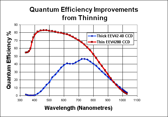
Even when photons enter the silicon, they don't always knock electrons into the conduction band. Some pass all the way though the chip without interacting; at wavelengths greater than 1 micron, silicon becomes nearly transparent. Moreover, some of the electrons are swallowed up by holes or impurities in the crystal. The bottom line is an overall quantum efficiency which varies across the visible spectrum. Some designs yield peak QEs close to 1.0, but they tend to be the most expensive.
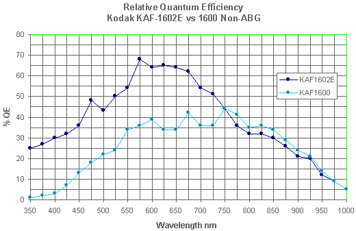
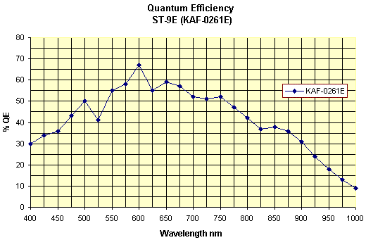
Back in the early 2000s, the RIT Observatory was equipped with a pair of cameras made by Santa Barbara Instruments Group (SBIG): the SBIG ST-8E camera had a Kodak KAF1602E chip in it, and our SBIG ST-9E camera had a Kodak KAF0216E chip. As you can see, the two have similar spectral response.
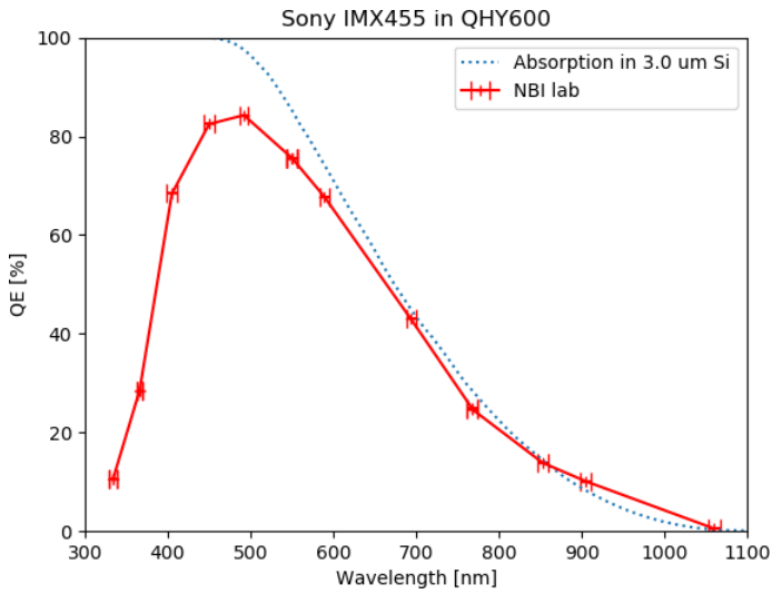
More recently, we've switched to a pair of cameras built around more recent (and larger) chips: first, the Atik 11000, features a CCD chip made by Kodak: the Kodak KAI-11002, monochrome version with microlenses. And our latest camera, which most of you will use, the ZWO ASI6200MM, is built around the Sony IMX455 CMOS sensor.
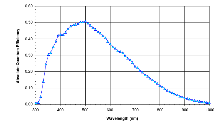
KAI data courtesy of
ON Semi datasheet ;
ASI6200MM data thanks to
Norup on cloudynight.
      Q: How does the quantum efficiency of our newer cameras
            compare to that of our older SBIG devices?


         In particular, a)  what is the peak sensitivity?

                        b)  at what wavelength is it most sensitive?

                        c)  how sensitive is it at 656 nm?
Under proper conditions, each photon which strikes a pixel produces a single electron. By counting electrons, we directly count incident photons. In other words, CCDs are linear devices: the output (electrons) is directly proportional to the input (photons). Not all detectors are linear: photographic film, for example, has a notoriously complex response to light which varies with intensity; it is linear over only a small range of incoming flux values.
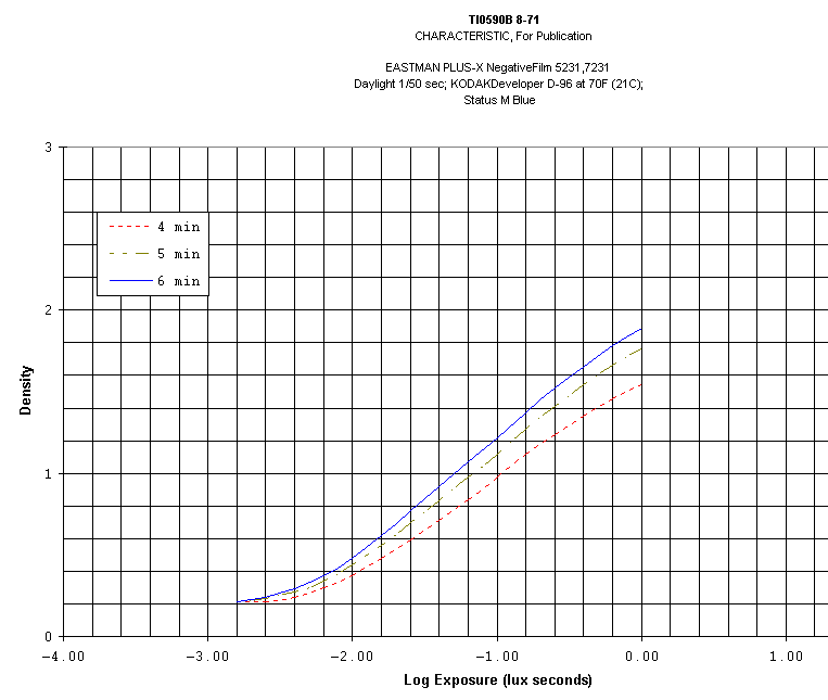
Most CCDs are very linear: the output is proportional to the input to a very high degree. If any non-linearity appears, it's usually only close to the very largest signal levels:
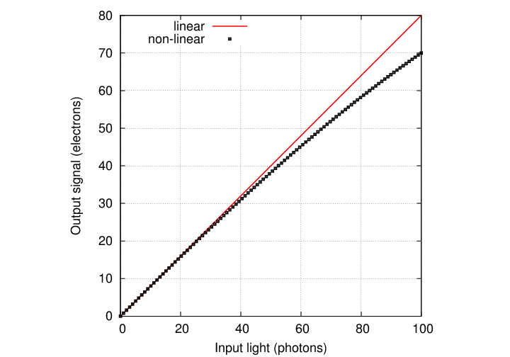
However, even CCDs start to distort the incoming signal when it becomes too large. When the number of electrons in a single pixel starts to approach the full-well capacity of the device, some of them are lost to inactive areas of the silicon or to neighboring pixels.
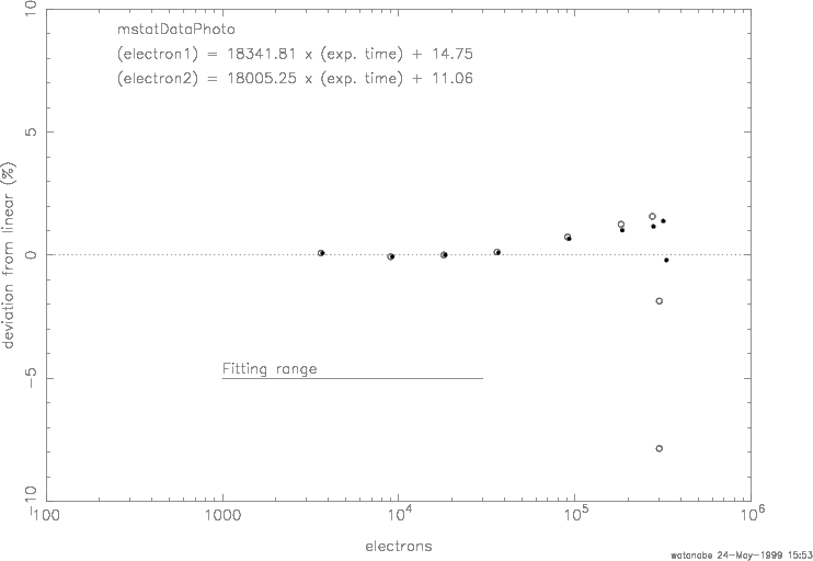
The gain on most CCDs is set so that the highest possible pixel value (65536 on RIT's camera) is near the full-well capacity; you should be wary of any values close to this limit. Below is a graph of the deviations from linear response for one of the 'z' CCD chips used in the Sloan Digital Sky Survey, as measured by Masaru Watanabe and Mamoru Doi. Note the horizontal axis has a logarithmic scale.
Since electrons don't need to be transferred across the chip in CMOS sensors, they don't suffer from the bleed trails described below. Only CCD-based cameras will show bleed trails.
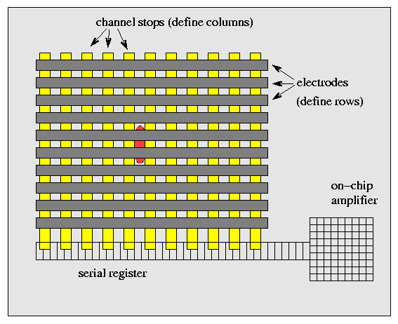
When the number of photons hitting a single pixel becomes much larger than the full-well depth, some of the pixels start to "bleed" into neighboring pixels in the same column:
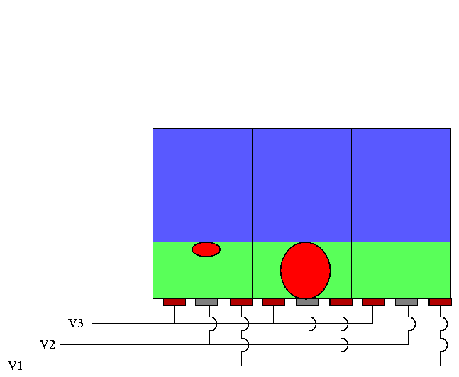
The channel stops prevent electrons from migrating across columns, so they move up and down along a column, leaving a "bleed trail":
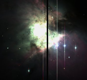
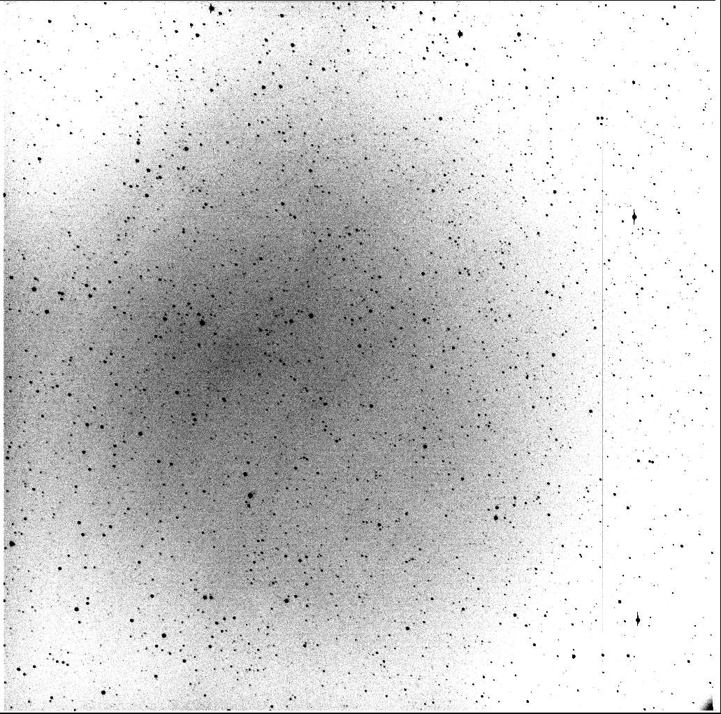
Here's an example of a CCD image with big bleed trails. There's not much one can do to avoid them when bright stars are embedded in faint nebulosity.
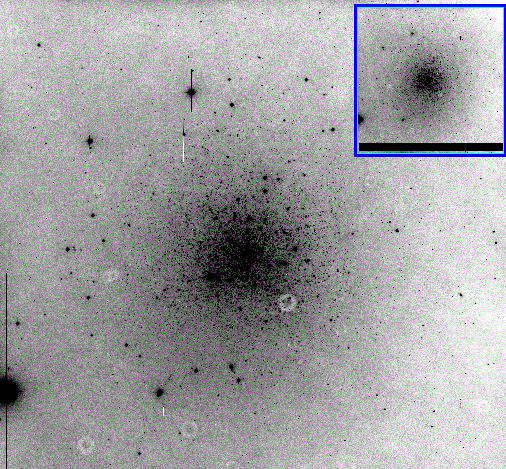
The example below shows some very nasty bleed trails in an image of the open cluster Trumpler 14, taken by HST.
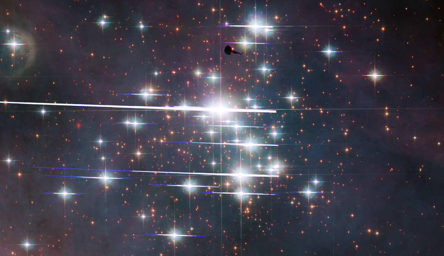
Image courtesy of
Judy Schmidt
Our ASI 6200MM camera does not show any strong dark current.
Thermal motions of the atoms in a silicon crystal can knock electrons into the conduction band. Astronomers call this signal the dark current, because it appears even when the shutter is closed and no light strikes the chip. Some spots in the crystal have defects which cause many electrons to be produced each second -- which lead to hot pixels.
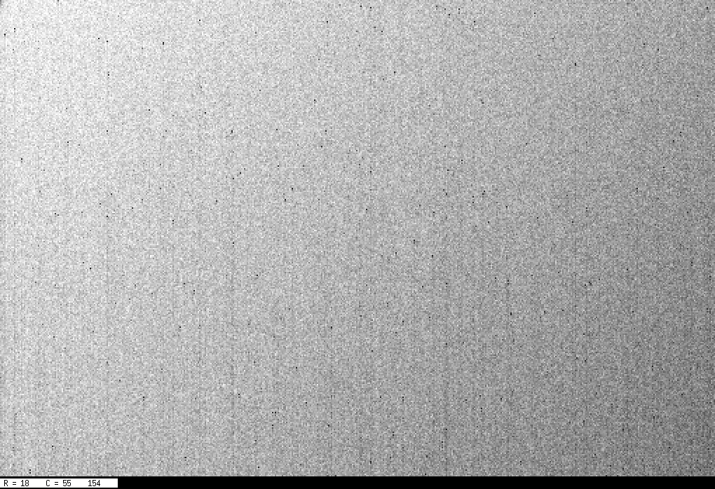
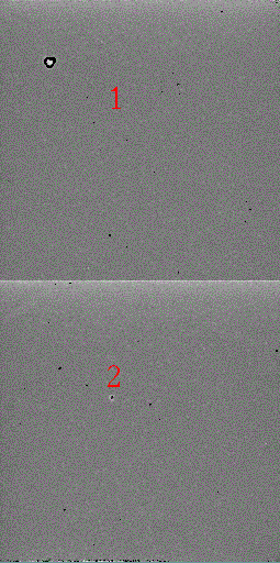
Here's a sample dark frame from an RIT CCD camera. The exposure time is only 0.12 seconds:
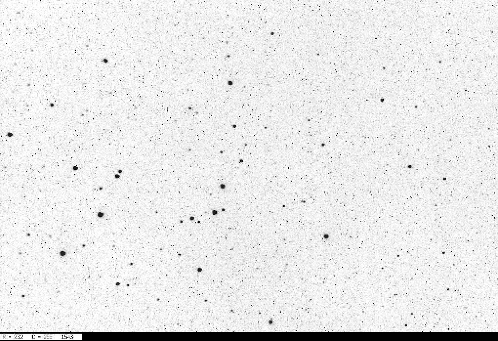
Another dark frame, 30 seconds in length, shows many more hot pixels.
How can one deal with this source of false signal?
Compare the raw 30-second image below with the same image after subtracting the "master dark frame". Click on the raw image to see the dark-subtracted version.
This next issue is a combination of the sensor itself, and the optics which bring light to a focus on it. The net result is a variation in sensitivity across the focal plane; if those variations are not corrected, they end up as errors in the measured magnitudes of stars and other celestial sources.
The three main culprits are
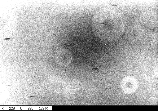
Here's an example: a raw I-band image taken by one of the TASS Mark IV cameras . The field of view is very large, about 4 degrees on a side.
You can download and examine the image itself, if you wish. Be careful, though: it's a big image, roughly 2048x2048.
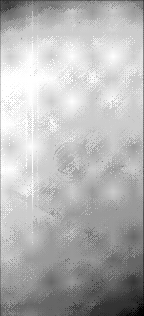
Some CCDs may have been nearly perfect when first made, but, over the years, have accumulated layers of oil, grease, or other contaminants. Little specks of dirt and dust can also sit on the chip, blocking most of the light from reaching the pixels below. Here are a couple of closeups of quadrants 1 and 2 of the Dandicam CCD camera.
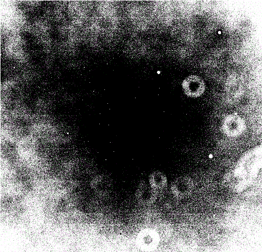
and the 1-m telescope at Las Campanas in Chile:
What do we see in images taken by our camera at the RIT Observatory? Why don't you find out?
The problem boils down to this: imagine a very simple CCD, consisting of just two pixels. Suppose that the pixel on the left is a bit less sensitive than that on the right. I point my camera at a blank white wall. I ought to see this:
             left pixel              right pixel
           --------------         ----------------
              100 counts             100 counts
But instead, the CCD actually records this:
             left pixel              right pixel
           --------------         ----------------
                95                      100
Evidently, the left-hand pixel is slightly less sensitive to light, by 5 percent. This is a problem if we're trying to make precise measurements of stellar brightness. Suppose I look at two stars, A and B, which are really the same brightness. But if star A falls on the left-hand pixel, and star B on the right-hand pixel, I won't see that; instead, I will measure fewer counts from star A:
              star A                   star B
           --------------         ----------------
               9,500                   10,000
      Q:  Is there any way to correct the measured quantities
             so that they accurately reflect the actual
             incoming signals from the stars?
Sure! It's not too hard, either. All I need to do is divide each pixel's measured value by its relative sensitivity, like this:
              star A                   star B
           --------------         ----------------
 measured      9,500                   10,000

            divided by              divided by

 relative
 sensitivity     0.95                    1.00

            ===========             ============

  corrected   10,000                   10,000
So, the theory of "flatfields" goes like this:
There are a few complications:
                 uncertainty = 1.0 / sqrt(100)

                             =  0.1   =  10 percent
If you want to do work at the 1 percent level,
you need to gather roughly 10,000 electrons
in each pixel of the flatfield image.
It's a bit more complicated than this, but a good rule of thumb is "take flatfield images which are around 1/4 to 1/2 of the saturation level." For the RIT cameras, anywhere between 10,000 and 28,000 counts per pixel is pretty good.
Fortunately, this is easy to fix: just take a set of dark frames with the same exposure time as your flatfield images, create a master dark, and subtract that master dark from all flatfield frames before any further processing.
The short horizontal streaks are due to stars which were bright enough to appear above the relatively bright sky level. They are trailed because the telescope's tracking was turned off (oops).
Again, there is a relatively simple solution: take a number (10 or more) of flatfield images, and (after subtracting the master dark from each one) create a "master flat" by taking the median of the set, on a pixel-by-pixel basis.
Copyright © Michael Richmond.
This work is licensed under a Creative Commons License.