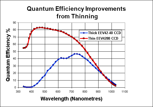
CCDs are not perfect detectors -- they do not record every single photon which strikes them. One reason is the change of index of refraction between air and the silicon itself.
Look at the chips below. Which chips absorb the largest amount of light?
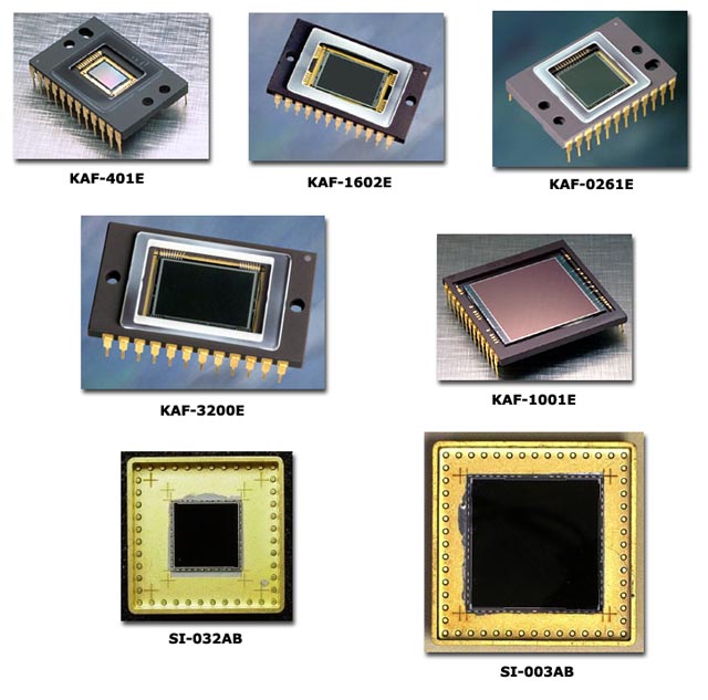
Images of CCD chips courtesy of
astrosurf.com
One can reduce reflective losses by anti-reflection coatings. The idea is to cause destructive interference between a light ray which bounces off the front surface of the coating (labelled "A" in the diagram below) and a light ray which bounces off the back surface of the coating. If we can arrange it so that these reflected light rays interfere correctly, we can in essence prevent such reflection from taking place.
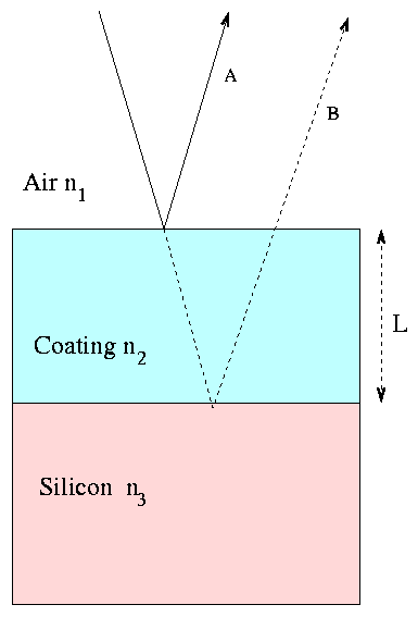
The first ray, "A", has its phase shifted by half a wavelength because it is bouncing off a material with higher refractive index than air. If we can cause the second ray, "B", to have an overall phase shift of zero, then the two rays will be perfectly out of phase and destroy each other.

So, in order to create destructive interference between rays "A" and "B", we want

and so

Note that one can arrange for perfect destructive interference only at a particular wavelength; there will be some reflection at other wavelengths. For CCDs, the designer typically chooses a wavelength near the middle of the visible band, around 550 nm. This EEV chip, on the other hand, had its reflectivity optimized for 400 nm.
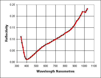
A good coating will have an index of refraction between that of air (n1 = 1.0) and silicon (n3 = 3.6). The best results occur when the coating's index is the square root of the silicon's: n2 ~ 1.9. One common choice is hafnium dioxide.
-
Even when photons enter the silicon, they don't always knock
electrons into the conduction band. Some pass all the way
though the chip without interacting;
at wavelengths greater than 1 micron, silicon becomes
nearly transparent.
Moreover, some of the electrons are swallowed up by holes
or impurities in the crystal.
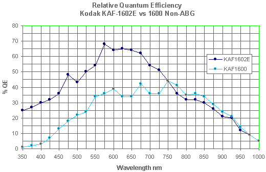
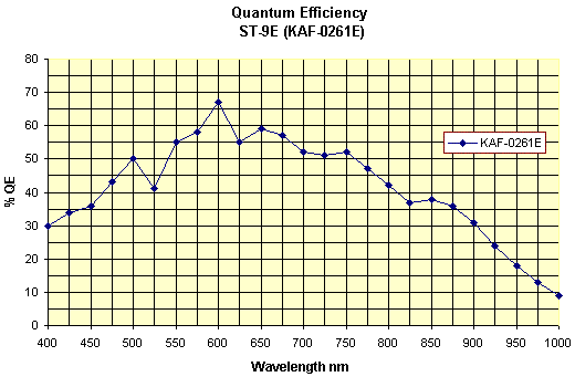
The bottom line is an overall quantum efficiency
which varies across the visible spectrum.
Some designs yield peak QEs close to 1.0, but they tend to
be the most expensive.
Our SBIG ST-8E camera has a Kodak KAF1602E chip in it, and our SBIG ST-9E camera has a Kodak KAF0216E chip. As you can see, the two have similar spectral response.
-
Under proper conditions,
each photon which strikes a pixel produces a single electron.
By counting electrons, we directly count incident photons.
In other words, CCDs are linear devices:
the output (electrons) is directly proportional to the input (photons).
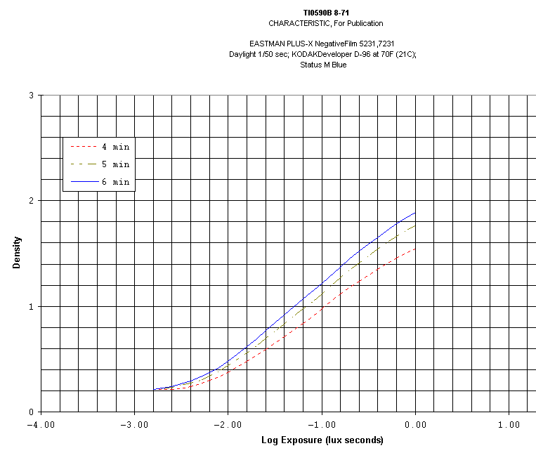
Not all detectors are linear:
photographic film, for example,
has a notoriously complex
response to light
which varies with intensity; it is linear
over only a small range of incoming flux values.
- Stars "A" and "B" have true magnitudes 10.0 and 13.0,
respectively.
You take an image which is long enough that the response
to star "A" is non-linear.
What would the difference in the instrumental
magnitudes be?
- less than 3.0 mag
- exactly 3.0 mag
- more than 3.0 mag
Most CCDs are very linear: the output is proportional to the input to a very high degree. If any non-linearity appears, it's usually only close to the very largest signal levels:
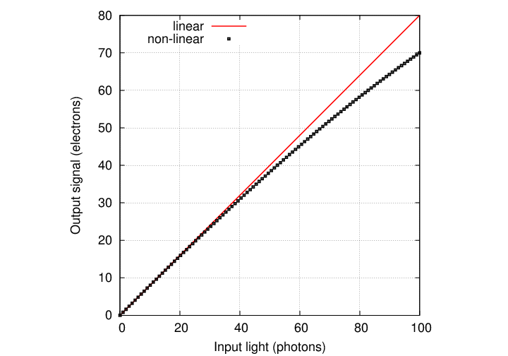
However, even CCDs start to distort the incoming signal when it becomes too large. When the number of electrons in a single pixel starts to approach the full-well capacity of the device, some of them are lost to inactive areas of the silicon or to neighboring pixels.

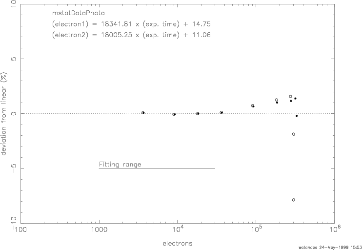
The gain on most CCDs is set so that the highest possible pixel value (65536 on RIT's camera) is near the full-well capacity; you should be wary of any values close to this limit. Below is a graph of the deviations from linear response for one of the 'z' CCD chips used in the Sloan Digital Sky Survey, as measured by Masaru Watanabe and Mamoru Doi.
Exercise:
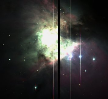
When the number of photons hitting a single pixel becomes much larger than the full-well depth, some of the pixels start to "bleed" into neighboring pixels in the same column:
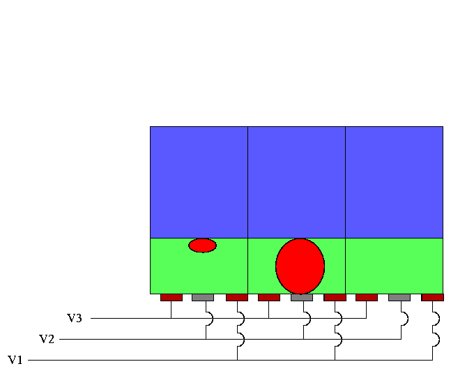
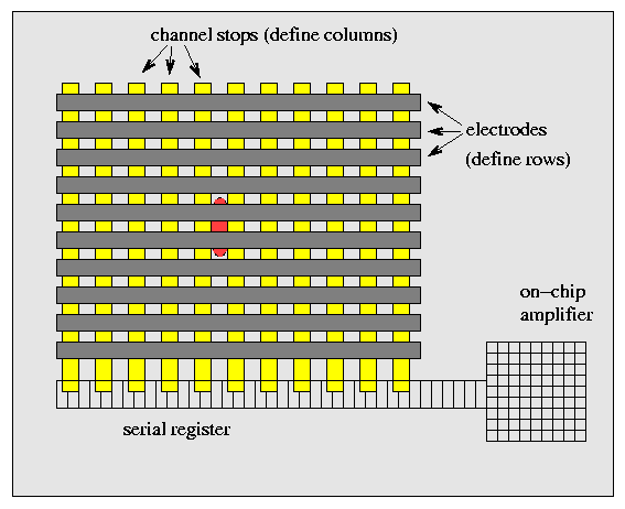
The channel stops prevent electrons from migrating across columns, so they move up and down along a column, leaving a "bleed trail":
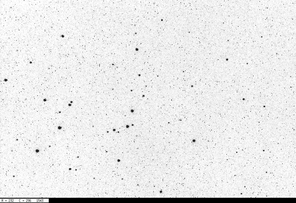
Here's an example of a CCD image with big bleed trails. There's not much one can do to avoid them when bright stars are embedded in faint nebulosity.
-
Thermal motions of the atoms in a silicon crystal
can knock electrons into the conduction band.
Astronomers call this signal the dark current,
because it appears even when the shutter is closed
and no light strikes the chip.
Some spots in the crystal have defects which
cause many electrons to be produced each second --
which lead to hot pixels.
- Cool the camera. For each drop of 5 degrees Celsius,
the dark current decreases by a factor of 2 or so.
Professional CCDs are cooled by liquid nitrogen
(which boils at 77 Kelvin).
We use a thermoelectric cooler to bring the chip
temperature to -10 degrees Celsius or so;
for short exposures in the bright Rochester skies,
this leads to a negligible
amount of noise from the dark current.
- Take a series of dark frames with exactly the same exposure time as your target frames. Combine the dark frames to make a single "master dark frame." Subtract this "master dark" from each target image. This should remove the signal in hot pixels (though it can't remove the noise caused by the dark current...)
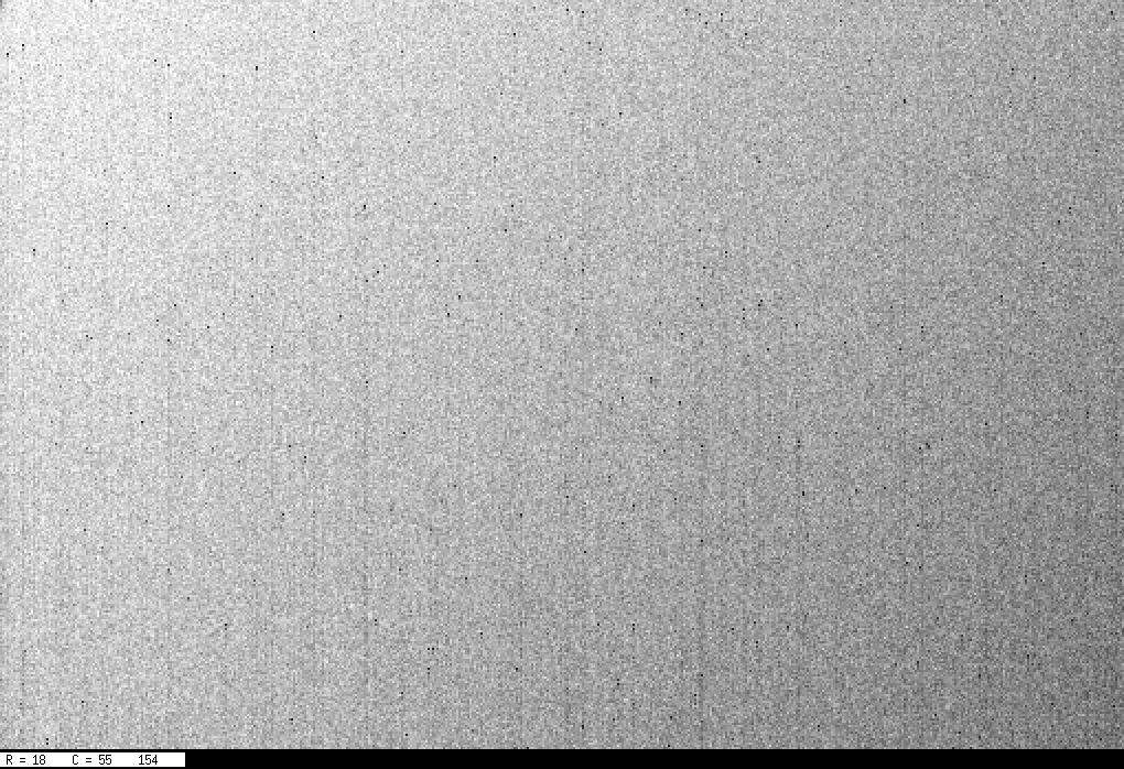
Here's a sample dark frame from the RIT CCD camera. The exposure time is only 0.12 seconds:
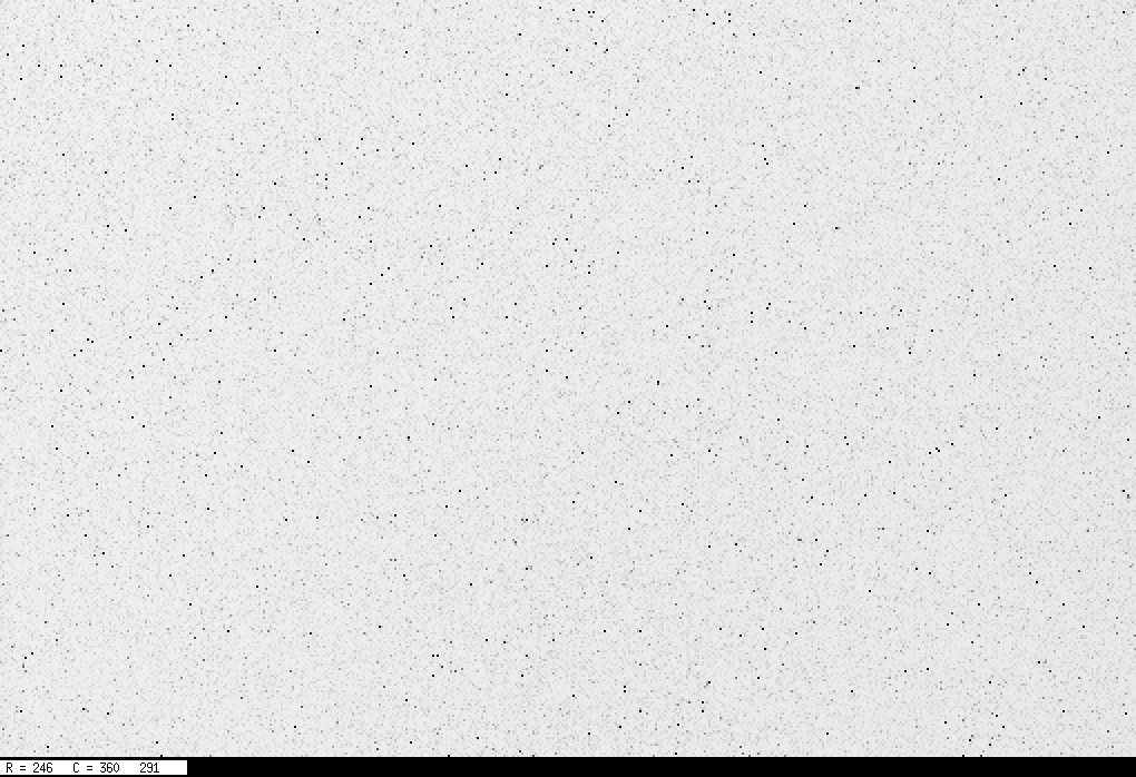
Another dark frame, 30 seconds in length, shows many more hot pixels.
How can one deal with this source of false signal?
Compare the raw 30-second image below with the same image after subtracting the "master dark frame". Click on the raw image to see the dark-subtracted version.
For more information
- The
Observational Mishaps
page contains examples of wierd and awful CCD images.
Some of them are due to problems with the chips themselves,
other due to optics, telescope motion, and so forth.
- Another set of CCD images with wierd problems can be found at Silicon Owl's CCD Probems page.
 Copyright © Michael Richmond.
This work is licensed under a Creative Commons License.
