 Copyright © Michael Richmond.
This work is licensed under a Creative Commons License.
Copyright © Michael Richmond.
This work is licensed under a Creative Commons License.
Ordinary microscopes focus light which is emitted (or reflected) from objects. The resolution of such a microscope is limited by the wavelength of light. Microscopes which employ visible light cannot resolve features smaller than about 500 nm. Individual atoms are much smaller than that -- just a few nanometers in diameter. Is there any way to resolve atomic features?
Yes -- but it involves a very different sort of microscope. The scanning tunneling microscope (or STM for short) relies on two physical principles you have seen in your physics courses:
Let's look at how each contributes to the STM.
Consider a particle with an energy less than that of a thin potential energy barrier.
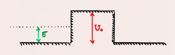
In the world of classical physics, the particle is forbidden from every crossing the barrier. But in the quantum world, there is a small probability that it may tunnel through the barrier to the other side.
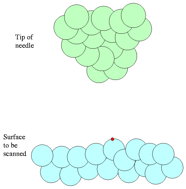
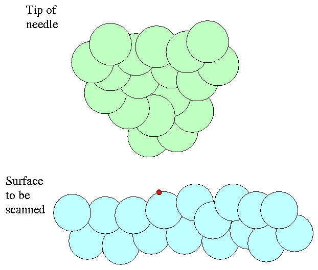
The STM contains a thin wire with a specially prepared tip which is just a few atoms wide. If we place the tip within a micrometer of the surface of a material, and apply a small positive potential to the tip, we create a potential energy barrier for electrons in the surface: an air gap which they don't have enough energy to cross.
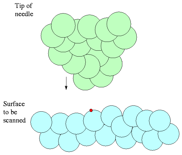
If we lower the tip towards the surface, we decrease the width of the barrier.

If we continue to lower the tip until it comes within a few nanometers of the surface,
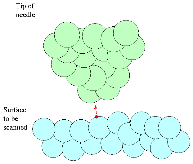
we finally make the barrier so thin that the electrons can tunnel through to the other side -- meaning that they can jump to the tip.
As they jump, we measure a current running through the wire. We can measure this current VERY accurately. Call that current I.
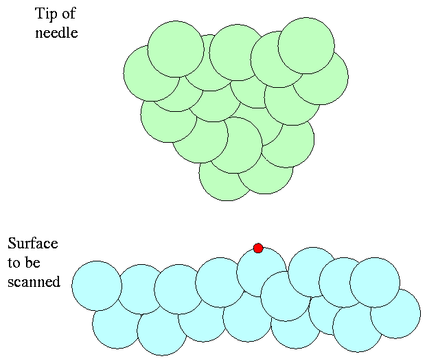
Now, if we slide the tip of the needle just a bit to the left, the exact distance between it and the surface may change a bit due to bumps and dips in the surface. In this example, the surface dips down just a fraction of an atomic diameter.

Even that fraction of a nanometer can significantly decrease the current through the wire, because the probability that electrons can tunnel through the barrier is a VERY sensitive function of its thickness:
                                    -2*k*x
  probability of tunneling  =  C * e
where x is the space between the surface and the tip,
and k is the wavenumber of the probability wave
in the region between the tip and surface.
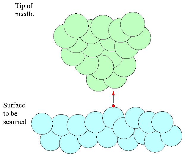
So, after sliding the tip sideways, our ammeter shows that the current has dropped from its previous value of I. We then drop the tip vertically by just enough
that the current regains its previous value I.
The distance we had to move the tip downwards is exactly the size of the dip in the surface. By repeatedly sliding the tip sideways a small distance, then raising or lowering the tip to maintain a constant current, we can build up a one-dimensional profile of the surface height. If we then shift the tip in the perpendicular direction and scan back again, we can measure a second profile, offset from the first by the width of the shift. Repeating the shifts and scans, over and over again, allows us to create a two-dimensional profile of the surface ... which, with the magic of image processing, can be turned into a pretty two-dimensional image.
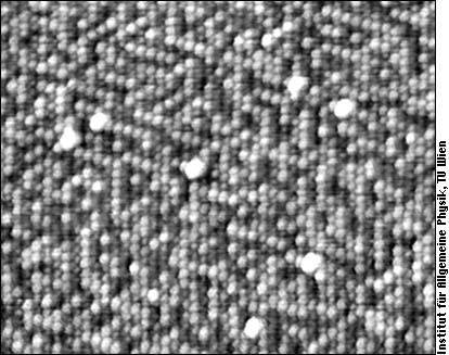
In this image, Pt (small dark spheres) and Ni (small lighter spheres) share about 50% of a metal surface. The white blobs in the image are impurities of unknown nature.
Now, one thing may be bothering you at this point: how can we possibly move the tip of the needle up, or down, or sideways, by a fraction of a nanometer? The answer isn't "tiny gears" ...
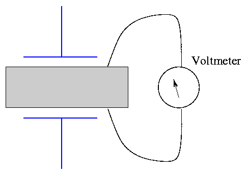
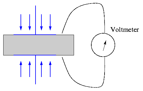
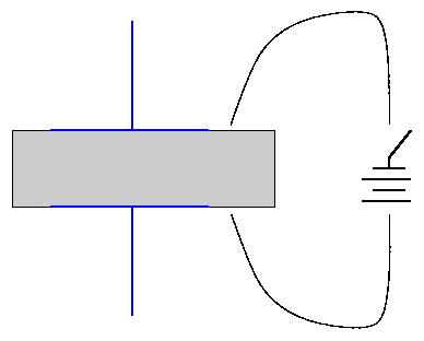
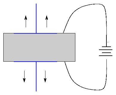
Some materials exhibit an effect called piezoelectricity, which means two things:
and/or
In pictures, squeezing the material produces a voltage:
or applying a voltage alters the material:
It turns out that you can purchase piezoelectric actuators which have will expand or contract by really small distances, given very reasonable voltages. Jurgen Muller's home-built STM, for example, uses the BM527 tube, which expands/contracts by 9 nm for every volt applied to it.
It's clear how one could use a piezoelectric device to move the tip of the needle up and down -- just glue the other end of the needle to a piezo oriented horizontally (as in the figures above). But what about moving the needle sideways?
It turns out that an elegant way to move the tip sideways for short distances (a few hundred nm) is to fasten two piezos to opposite sides of the harness holding the wire:
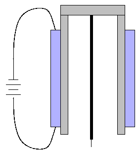
By varying the voltage applied to the left-hand piezo, one can cause the left-hand side of the harness to expand or contract a small amount. If the right-hand side remains fixed in length, then the needle held between them will tilt a bit. Very small angular tilts result in (nearly) horizontal motion of the tip.

Muller's STM bends so that the tip moves about 30 nm per volt of applied voltage.
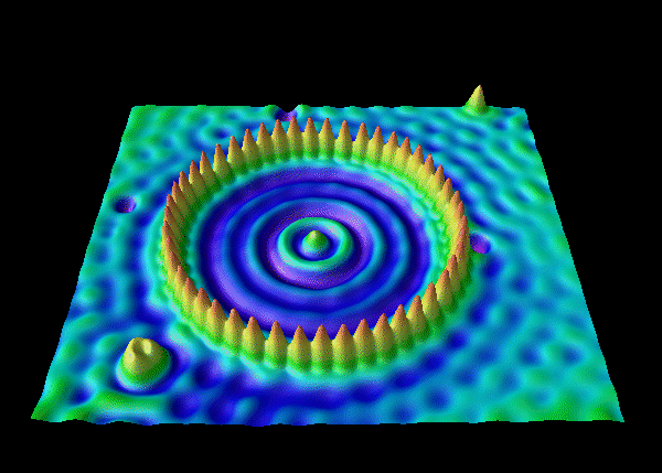
From IBM's "STM Image Gallery":
Here they have positioned 48 iron atoms into a circular ring in order to "corral" some surface state electrons and force them into "quantum" states of the circular structure. The ripples in the ring of atoms are the density distribution of a particular set of quantum states of the corral. The artists were delighted to discover that they could predict what goes on in the corral by solving the classic eigenvalue problem in quantum mechanics -- a particle in a hard-wall box.
First, a view from the top:
Now, take a look from the side, just peeking over the tips of the iron atoms:

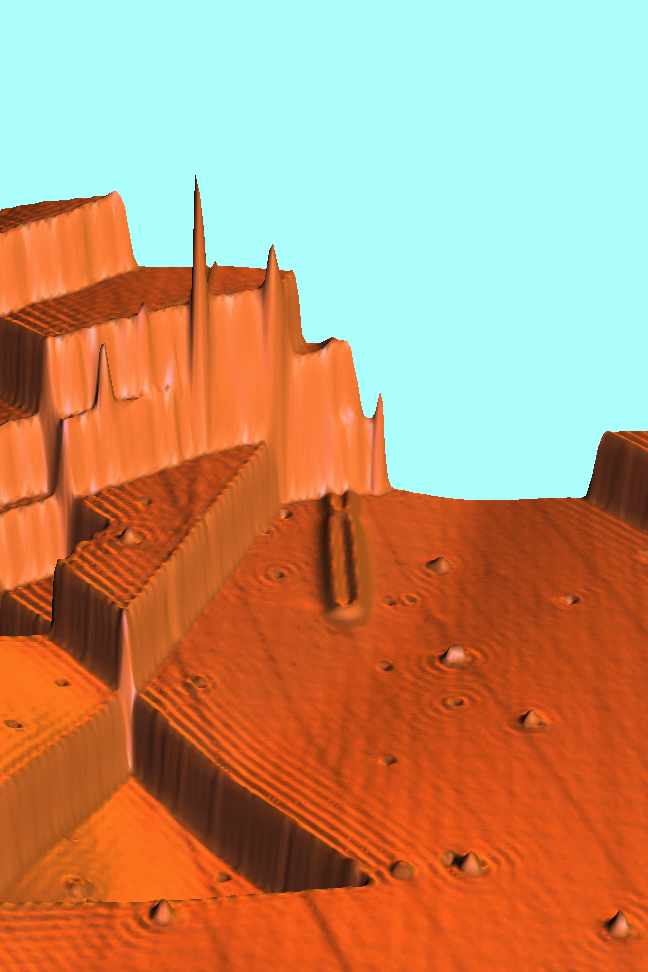
Reminiscent of formal Japanese rock gardens, here we see ripples surrounding features on the copper (111) surface. The artists' fortunes took a major turn upward when they determined that the ripples were due to "surface state electrons." These electrons are free to roam about the surface but not to penetrate into the solid. When one of these electrons encounters an obstacle like a step edge, it is partially reflected. The ripples extending away from the step edges and the various defects in the crystal surface are just the standing waves that are created whenever a wave scatters off of something. The standing waves are about 15 Angstroms (roughly 10 atomic diameters) from crest to crest. The amplitude is largest adjacent to the step edge where it is about 0.04 Angstroms from crest to trough.

Too cheap to buy a kit? There are many sites which will tell you how to do it all yourself:
Copyright © Michael Richmond.
This work is licensed under a Creative Commons License.