 Copyright © Michael Richmond.
This work is licensed under a Creative Commons License.
Copyright © Michael Richmond.
This work is licensed under a Creative Commons License.
Electronic circuits control many aspects of our modern lives. Some of them are quite complicated. Even simple circuits with ten or twenty elements can become messy if one tries to put them together with wires ...

... so engineers figured out decades ago to construct special integrated circuits with all the pieces and connections pre-made on a single chip. Just a few small wires attached to the chip can carry currents and measure voltages.
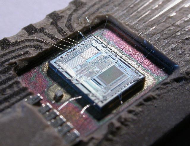
A large-scale integrated circuit can contain millions of individual electrical gates and wires and components (the example below has just a few hundred).
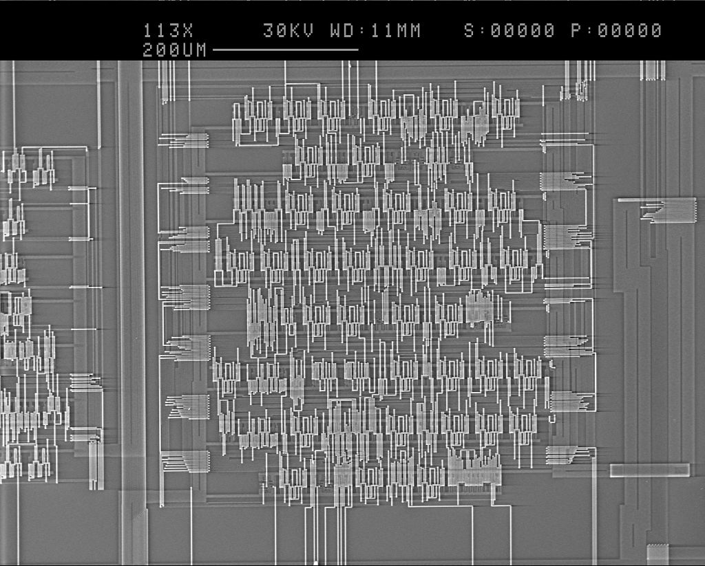
Each individual "wire" and "connection" may be just a fraction of a millionth of a meter wide:
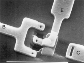
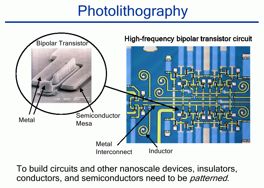
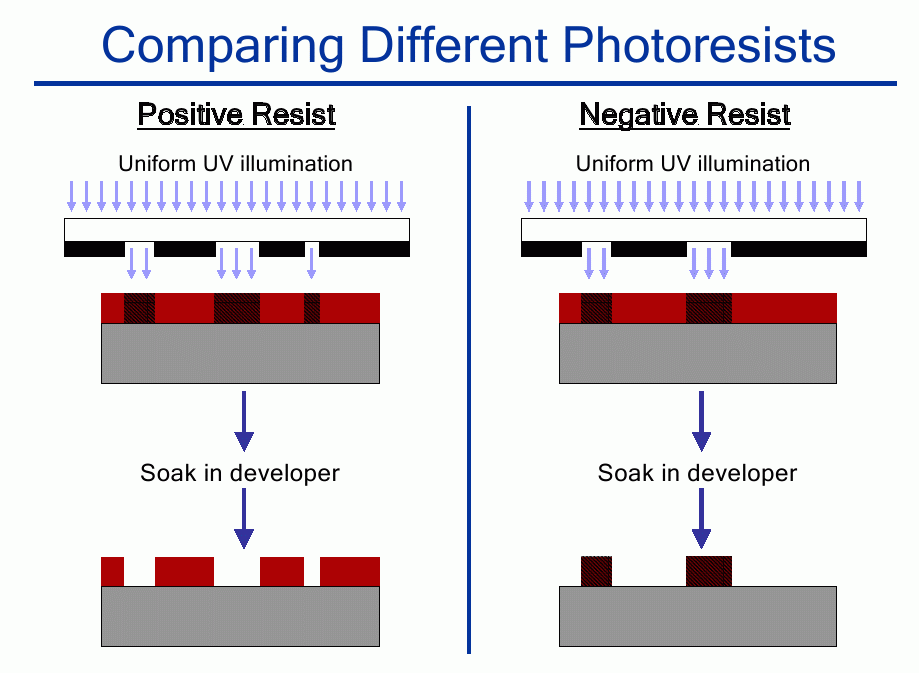
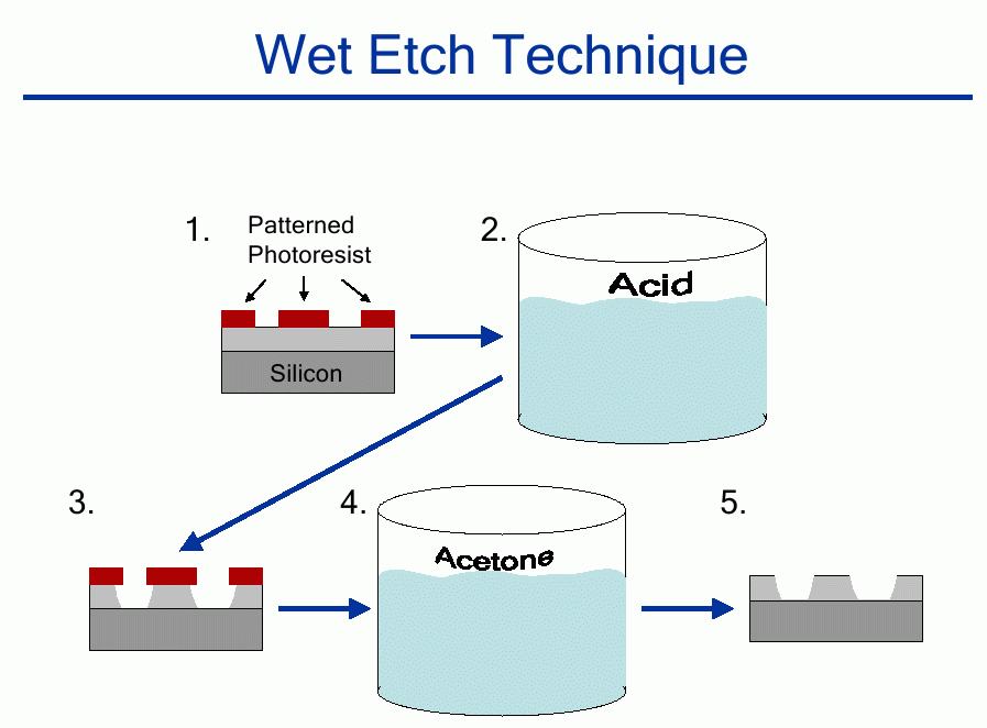
How can one construct circuits with such fine detail? The answer is photolithography, which is a fancy word for "printing with light". Here's the basic idea -- thanks for the pictures to a presentation by Ilan Ben-Yaacov from UC Santa-Barbara
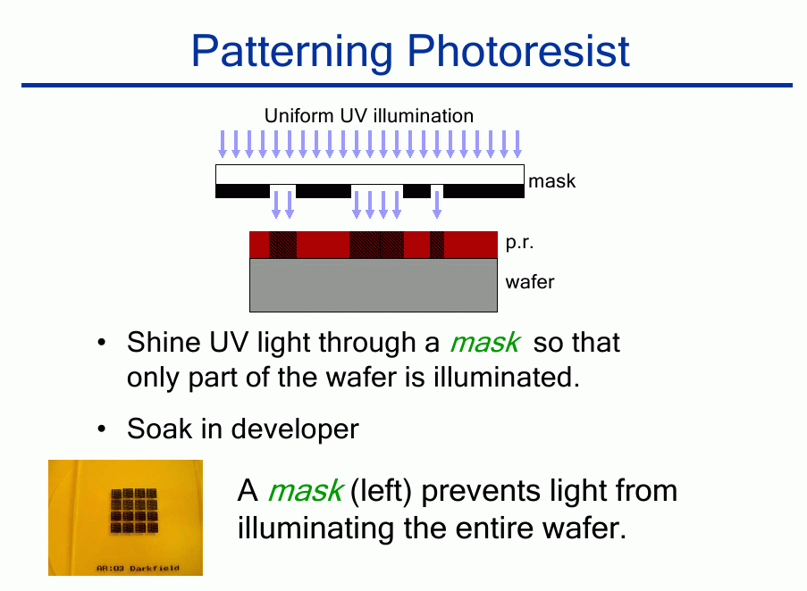
One of the crucial steps in this process involves shining light through a mask with a complicated series of holes. That, unfortunately, allows diffraction to come into the picture.
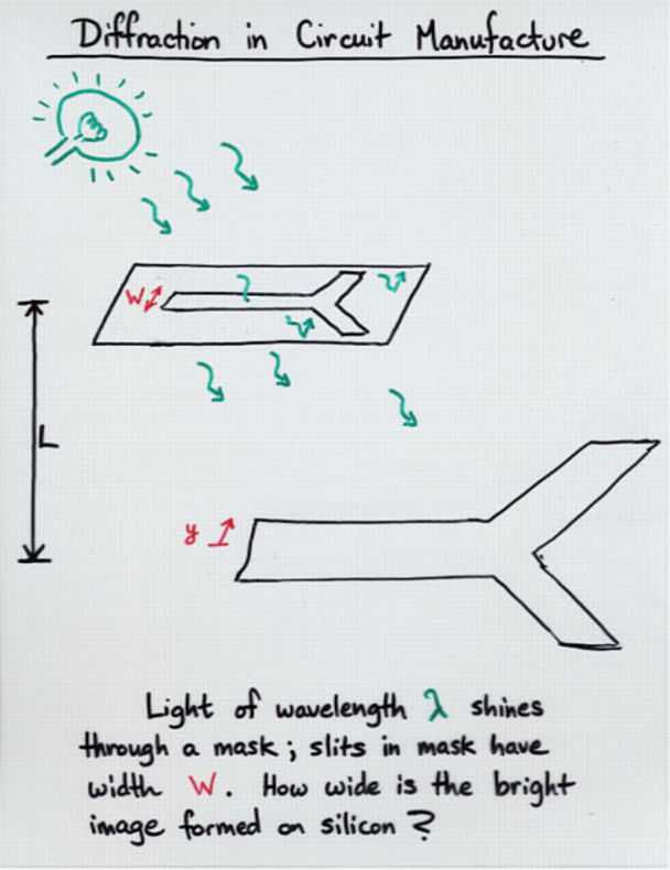

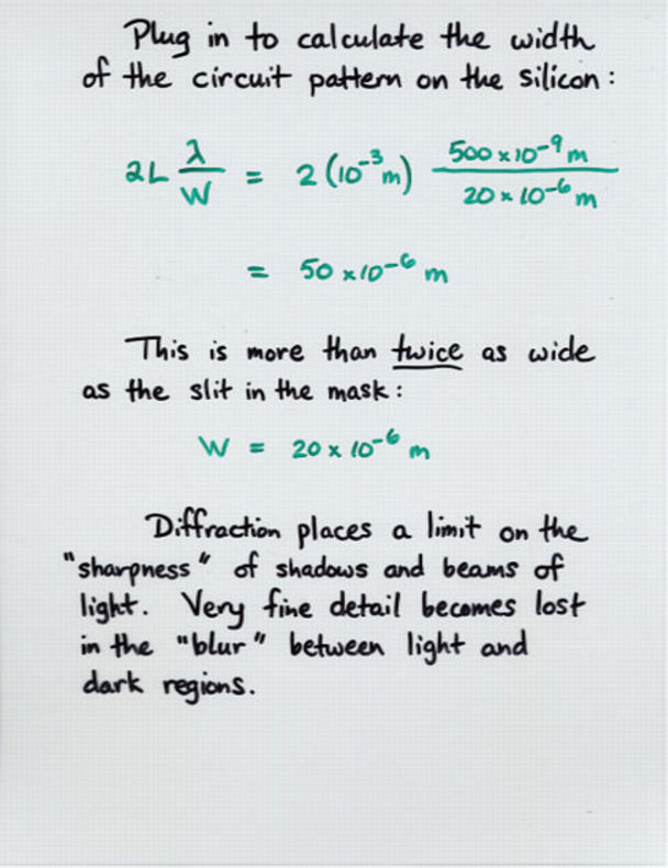
As one tries to cram more and more components into a single chip, one needs to make each piece smaller and smaller ... but diffraction causes the edges of the pattern cast by the mask to blur.
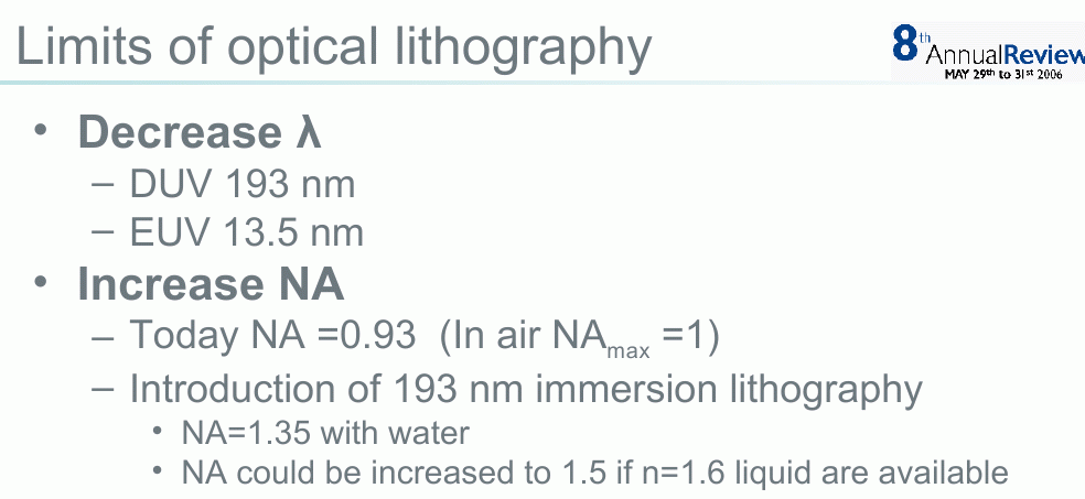
  Q:  How can one improve the sharpness
      of the image projected on the wafer?
There are many possibilities, but two of the most common ones are
Thanks to
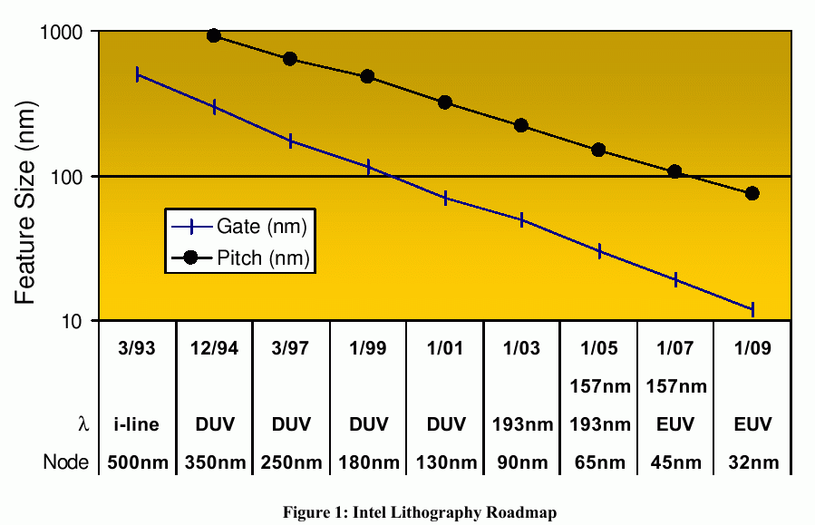
S. Tedesco's Lithography Roadmap
Manufacturers have been decreasing the wavelength of light sent through their masks for years. This figure is part of a presentation made in 2002 by the Intel Corporation.
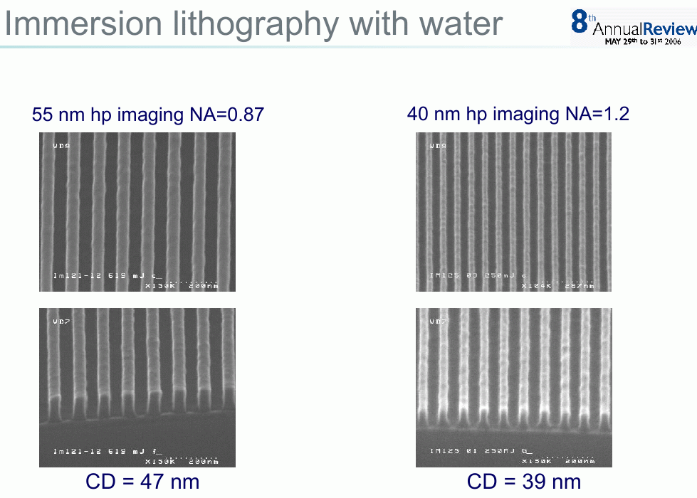
Creating and focusing UV light is not always easy. One way to avoid generating very short UV light is to immerse the mask and target in a liquid, so that the wavelength of light shrinks before it reaches the target. This "immersion" procedure shows promise:
Update -- progress through 2011
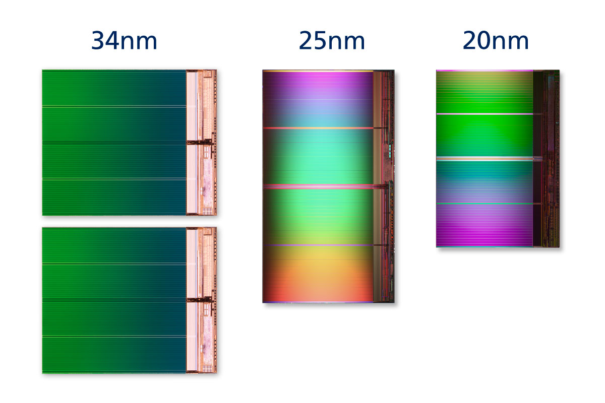
Intel and Micron are currently producing NAND memory chips with a 20-nm process. The chip at right is about 15 mm long.
Moreover, Intel is planning to continue work on immersion processing using regular UV (not the shorter wavelength EUV -- yet). The new technique -- which won't used in production for a few years -- should permit the construction of 11 nm traces!
  If a trace is 11 nm wide, how many atoms
  does it take to go from left to right
  across the trace?
Copyright © Michael Richmond.
This work is licensed under a Creative Commons License.